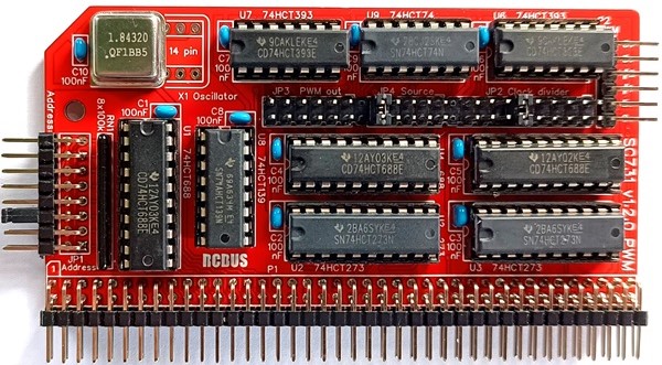
SC731 is a two channel Pulse Width Modulation signal generator.
- SC731 – Assembly guide
- SC731 – Compatibility
- SC731 – Parts list
- SC731 – Printed circuit board
- SC731 – User guide
- SC700 series information
- SC700 series support
Downloads
- SC731, v1.2, Kit contents sheet (PDF)
- SC731, v1.2, Schematic (PDF)
- SC731, v1.2, PCB design files (OSHWLab)
- SC731, v1.2, Gerber files (ZIP)
Errata
Nothing known
Suppliers
| Kits | Website | From | Currency |
| Small Computers Direct | SCDirect | UK | GBP |
| Stephen C Cousins | Tindie | UK | USD |
| Small Computer Central | Lectronz | UK | Euro/USD |
| PCBs | Website | From | Currency |
| Small Computers Direct | SCDirect | UK | GBP |
| Stephen C Cousins | Tindie | UK | USD |
| Small Computer Central | Lectronz | UK | Euro/USD |
| Assembled and Tested | Website | From | Currency |
| Not available | |||
| Components | |||
| See parts list |
Tindie does not collect VAT for EU countries
Lectronz does collect EU VAT for orders up to 150 EUR
Parts List
| Reference | Qty | Component |
| PCB | 1 | SC731, v1.0, PCB |
| C1 to C10 | 10 | Capacitor, ceramic, 100 nF |
| JP1 | 1 | Header, male, 2 x 8 pin, angled |
| JP2 | 1 | Header, male, 2 row x 9 pin, straight |
| JP3 | 1 | Header, male, 2 row x 6 pin, straight |
| JP4 | 1 | Header, male, 2 row x 5 pin, straight |
| Jumper | 10 | Jumper shunt |
| P1 | 1 | Header, male, 2 row x 40 pin, angled |
| P2 | 1 | Header, male, 1 x 6 pin, angled |
| RN1 | 1 | Resistor network, 8x100k, SIL, 9-pin |
| Screw (for spacer) | 1 | Machine screw, 6mm, M3 |
| Spacer | 1 | Spacer, 10mm, M3, nylon |
| U1, U4, U5 | 3 | 74HCT688 |
| U2, U3 | 2 | 74HCT273 |
| U6, 7 | 2 | 74HCT393 |
| U8 | 1 | 74HCT139 or 74AHCT139 |
| U9 | 1 | 74HCT74 |
| X1 | 1 | Oscillator 1.8432 MHz |
| IC socket 20-pin U1 to U5 | 5 | Socket, DIP, 20-pin |
| IC socket 16-pin U8 | 1 | Socket, DIP, 16-pin |
| IC socket 14-pin U6, U7, U9, X1 | 4 | Socket, DIP, 14-pin |
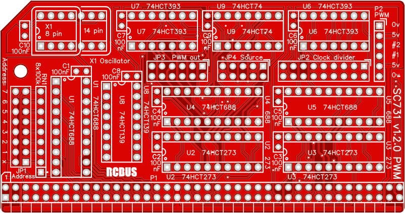
Printed Circuit Board
User Guide
SC731 is a two channel Pulse Width Modulation signal generator. It has tight address decoding and easy access with a single OUT instruction to set each PWM output.
The address decoding is such that one module takes only two I/O addresses (one for each PWM channel). Only writes to those addresses are decoded, so those addresses could be allocated to another device that only has a read function. Many of these modules can be installed in a single system as long as there are no address conflicts.
The output of each channel is set by writing a value from 0 to 128 decimal to the port address of the PWM channel. A value of zero turns the pulses off, leaving the output signal at a steady low level. A value of 128 turns the output constantly on with the output signal at a steady high level. A value of 1 produces the most narrow pulse and 127 the most wide pulse.
The frequency of the pulses is determined by the Clock frequency set with JP2. The frequency of the pulses is Clock/128.
Examples
If the base I/O address is set to 4, then to set the value of the PWM #1 pulse width you need to write the value to I/O address 4. PWM #2 width is set at I/O address 5.
To set the width of PWM #1 channel to 100 (decimal) in BASIC:
OUT 4, 100
To set the width of PWM #1 channel to 100 (decimal) in assembler:
LD A, $64
OUT (4), A
Input/output port functions
| RCBus I/O Address | Read | Write |
| Configurable *1 base address | n/a | Write PWM value |
- The RCBus I/O address should be set to any even address. Typically, this might be 0x04 (4 decimal). Many of these modules can be included in a single system as long as there are no address conflicts.
Jumper options
| Jumper | Function |
| JP1 | Set SC731’s RCBus I/O base address SC731 takes two I/O addresses: PWM #1 is at the base address PWM #2 is at the base address + 1 |
| JP2 | Set clock divider for both PWM channels JP 2.1 Clock is source/256 JP 2.2 Clock is source/128 JP 2.3 Clock is source/64 JP 2.4 Clock is source/32 JP 2.5 Clock is source/16 JP 2.6 Clock is source/8 JP 2.7 Clock is source/4 JP 2.8 Clock is source/2 JP 2.9 Clock is source Only fit one jumper shunt to this set of jumper pins The PWM frequency is Clock/128 |
| JP3 | Connect PWM outputs to bus pins JP 3.1 Connect PWM1 output to bus CLK2 (pin 61) JP 3.2 Connect PWM1 output to bus CLK3 (pin 40) JP 3.3 Connect PWM1 output to bus CLK4 (pin 80) JP 3.4 Connect PWM2 output to bus CLK2 (pin 61) JP 3.5 Connect PWM2 output to bus CLK3 (pin 40) JP 3.6 Connect PWM2 output to bus CLK4 (pin 80) |
| JP4 | Set clock source for both PWM channels JP 4.1 Clock is bus CLK signal (pin 21) JP 4.2 Clock is bus CLK2 signal (pin 61) JP 4.3 Clock is bus CLK3 signal (pin 40) JP 4.4 Clock is bus CLK4 signal (pin 80) JP 4.5 Clock is the on board oscillator X1 Only fit one jumper shunt to this set of jumper pins |
Frequencies
The following tables give the frequencies for each jumper #2 and jumper #4 position. The tables assume the on-board oscillator is 1.8432 MHz and the bus CLK signal is 7.3728 MHz. The signal named ‘Clock’ is used to count the pulse width, up to a maximum of 128. Therefore, the PWM signal frequency is Clock/128.
| JP 4 | Source | Frequency |
| 1 | Bus CLK (pin 21) | 7372800 Hz |
| 2 | Bus CLK2 (pin 61) | CLK2 |
| 3 | Bus CLK3 (pin 40) | CLK3 |
| 4 | Bus CLK4 (pin 80) | CLK4 |
| 5 | Fosc (X1) | 1843200 Hz |
With JP4 in position 5, the clock source is oscillator X1 which is assumed to be 1.8432 MHz, giving the following frequencies.
| JP 2 position | Clock divider | Clock frequency | PWM frequency |
| 1 | 256 | 7200 Hz | 56.25 Hz |
| 2 | 128 | 14400 Hz | 112.5 Hz |
| 3 | 64 | 28800 Hz | 225 Hz |
| 4 | 32 | 57600 Hz | 450 Hz |
| 5 | 16 | 115200 Hz | 900 Hz |
| 6 | 8 | 230400 Hz | 1800 Hz |
| 7 | 4 | 460800 Hz | 3600 Hz |
| 8 | 2 | 921600 Hz | 7200 Hz |
| 9 | 1 | 1843200 Hz | 14400 Hz |
With JP4 in position 1, the clock source is bus signal CLK which is assumed to be 7.3728 MHz, giving the following frequencies.
| JP 2 position | Clock divider | Clock frequency | PWM frequency |
| 1 | 256 | 28800 Hz | 225 Hz |
| 2 | 128 | 57600 Hz | 450 Hz |
| 3 | 64 | 115200 Hz | 900 Hz |
| 4 | 32 | 230400 Hz | 1800 Hz |
| 5 | 16 | 460800 Hz | 3600 Hz |
| 6 | 8 | 921600 Hz | 7200 Hz |
| 7 | 4 | 1843200 Hz | 14400 Hz |
| 8 | 2 | 3686400 Hz | 28800 Hz |
| 9 | 1 | 7372800 Hz | 57600 Hz |
With JP4 in position 2, 3 or 4, the clock source is bus signal CLK2, CLK3 or CLK4 respectively, giving the following frequencies.
| JP 2 position | Clock divider | Clock frequency | PWM frequency |
| 1 | 256 | CLK#/256 | CLK#/32768 |
| 2 | 128 | CLK#/128 | CLK#/16384 |
| 3 | 64 | CLK#/64 | CLK#/8192 |
| 4 | 32 | CLK#/32 | CLK#/4096 |
| 5 | 16 | CLK#/16 | CLK#/2048 |
| 6 | 8 | CLK#/8 | CLK#/1024 |
| 7 | 4 | CLK#/4 | CLK#/512 |
| 8 | 2 | CLK#/2 | CLK#/256 |
| 9 | 1 | CLK# | CLK#/128 |
Assembly Guide
Below is the suggested order of assembly. A general guide to assembling circuit boards can be found here.
- Decoupling capacitors C1 to C10
These can be fitted either way around - Header pins P2
- Sockets for U1 to U9
Fit such that the notch in the socket matches the curve in the outline on the PCB silkscreen - Socket for X1 (optional)
Not recommended as the oscillator is quite large and could touch other modules - Resistor network RN1
This must be fitted the correct way around whereby the dot on the component matches the dot on the PCB silkscreen - Bus header P1
Make sure the pins are parallel to the PCB so that the board is vertical when it is fitted into a backplane socket - Header pins JP1
- Header pins JP2, JP4 and JP4
These can be fitted as three separate strips or as a single strip with some pins pulled out - Insert the integrated circuits into their sockets
Make sure the notch in the component is at the end indicated by the notch in the socket and the curve on the PCB silkscreen - Fit oscillator X1
- Fit the nylon spacer in the mounting hole
Fit jumper shunts in the positions shown below. All other jumpers are optional and should only be fitted if the feature is required.
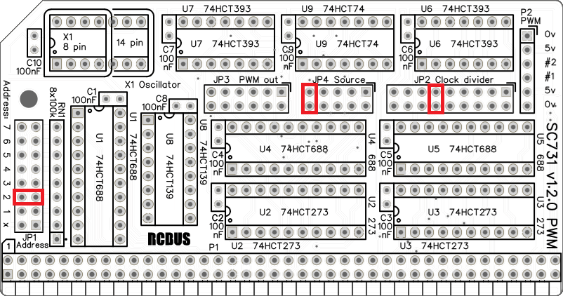
and the clock frequency is Fosc/8 (1.8432MHz/8 = 1800Hz)
Compatibility
This module conforms to the RCBus specification v1.0 for RCBus-2014 and RCBus-Z80.
The RCBus specification includes RCBus-2014 (both RC2014 standard 40-pin bus and RC2014 enhanced 60-pin bus) and also the full 80-pin RCBus. The 80-pin RCBus provides support for advanced Z80 features, such as the interrupt daisy-chain, as well as support for other processor families.
The table below indicates electrical compatibility with each backplane type (40, 60 and 80 pin)

| Backplane | ? | Compatibility notes |
| RCBus 80-pin |  | Fully supported |
| RCBus 60-pin (RC2014 enhanced) | | Limitations: Optional signal CLK4 not usually available |
| RCBus 40-pin (RC2014 standard) | | Limitations: Some optional signals are not available (CLK2, CLK4) |
The following table indicates electrical compatibility with SC731. Check firmware and software details for any required software support.
| Product (80-pin) | ? | Compatibility notes |
| SC126 Z180 motherboard | | Adds Z180 SBC motherboard |
| SC701 Backplane 6+1 | | Adds 6 module sockets RCBus 80-pin |
| SC702 Backplane 6+1 | | Adds 6 module sockets RCBus 80-pin |
| SC703 Power from 12v | | Adds power supply 8 to 15 volts input |
| SC704 I2C bus master | | Adds I2C bus master and I2C EEPROM |
| SC705 Serial ACIA | | Adds one serial port Typically set to 0x40 |
| SC706 Z80 CPU | | Adds Z80 CPU and clock oscillator |
| SC707 Memory 128k | | Adds 128kB RAM and 128kB ROM |
| SC708 Z80 SBC | | Adds single board Z80 computer |
| SC709 Backplane 12+1 | | Adds 12 module sockets RCBus 80-pin |
| SC710 Backplane 12+1 | | Adds 12 module sockets RCBus 80-pin |
| SC711 Prototyping | | Prototyping module |
| SC712 Power from 5v | | Adds power supply 5 volts input |
| SC713 RCBus tool | n/a | Simple reference tool No electrical function |
| SC714 Memory 512k | | Adds 512kB RAM and 512kB flash ROM |
| SC715 Compact flash | | Adds Compact Flash storage |
| SC716 Z80 SIO/2 | | Adds two serial ports Typically set to 0x84 |
| SC717 Z80 PIO | | Adds parallel I/O using Z80 PIO |
| SC718 Z80 CTC | | Adds counter/timer using Z80 CTC |
| SC719 Digital I/O | | Adds digital I/O Eight in, eight out |
| SC720 Z80 motherboard | | Adds Z80 SBC motherboard |
| SC721 Memory 512k | | Adds 512kB ROM and 512kB RAM |
| SC722 Z180 CPU | | Adds Z180 CPU and serial ports |
| SC723 Backplane 3 | | Adds 3 module sockets RCBus 80-pin |
| SC724 Breakout | | Prototyping breakout module |
| SC725 SIO+CTC | | Adds two serial ports and 4 counter/timers |
| SC726 Clock generator | | Generates CLK and CLK2 bus signals |
| SC727 Real time clock | | Adds real time clock for time and date |
| SC728 Module riser | | Simple module riser for RCBus 80-pin |
| SC729 Compact flash | | Adds Compact Flash storage |
| SC730 Z80 CPU + MMU | | Adds Z80 CPU with clock and MMU |
| SC731 Dual PWM generator | | Multiple modules can be used |
| SC732 Dual servo controller | | Adds dual servo controller |
| SC791 Z80 system | | Adds modular Z80 computer |
| SC792 Z180 system | | Adds modular Z180 computer |
| Product (40 pin) | ? | Compatibility notes |
| SC114 Z80 motherboard | | Adds Z80 SBC motherboard Some clock pins not available |
| SC130 Z180 motherboard | | Adds Z180 SBC motherboard Some clock pins not available |
| SC133 Backplane 11+1 | | Adds 11 module sockets RCBus 40-pin Some clock pins not available |
| SC134 LED output port | | Adds eight LED outputs |
| SC135 Digital output port | | Adds eight digital outputs |
| SC136 Digital input port | | Adds eight digital inputs |
| SC137 I2C bus master | | Adds I2C bus master |
| SC139 Serial ACIA | | Adds one serial port Typically set to 0x40 |
| SC141 Backplane 12+1 | | Adds 12 module sockets RCBus 40-pin Some clock pins not available |
| SC142 Power from 12v | | Adds power supply 8 to 15 volts input |
| SC143 Flash ROM | | Adds 128kB ROM in four 32kB banks |
| SC145 Compact flash | | Adds Compact Flash storage |
| SC147 Backplane 6+1 | | Adds 6 module sockets RCBus 40-pin |
| SC148 Power from 5v | | Adds power supply 5 volts input |
| SC149 Z80 CPU | | Adds Z80 CPU and clock oscillator |
| SC150 Paged RAM 128k | | Adds 128kB RAM in two 64kB banks |
| SC151 Paged ROM 128k | | Adds 128kB ROM in four 32kB banks |
| Other suppliers | ? | Compatibility notes |
| RC2014 Mini system | | Adds Z80 SBC motherboard Some clock pins not available |
| RC2014 Pro system | | Adds modular Z80 computer |
| RC2014 Zed system | | Adds modular Z80 computer |
| RC2014 Micro module | | Adds Z80 SBC computer |
| RC2014 Backplane 5 | | Adds 5 module sockets RCBus 40-pin |
| RC2014 Backplane 8 | | Adds 8 module sockets RCBus 40-pin |
| RC2014 Backplane Pro | | Adds 12 module sockets RCBus 60-pin |
| RC2014 Z80 CPU | | Adds Z80 CPU module |
| RC2014 SIO/2 dual serial | | Adds two serial ports at address 0x80 to 0x87 |
| RC2014 Compact flash | | Adds Compact Flash storage |
| RC2014 Dual clock | | Generate CLK2 only Conflict on CLK signal |
| RC2014 Pageable ROM | | Adds pageable ROM module |
| RC2014 64k RAM | | Adds pageable RAM module |
| RC2014 Memory 512k | | Adds 512kB RAM and 512kB flash ROM |
| RC2014 Digital I/O | | Adds eight LED outputs and eight push buttons |
| RC2014 Real time clock | | Adds real time clock for time and date |
| RC2014 RP2040 VGA terminal | | Connect VGA monitor and USB keyboard |
| RC2014 Pi Pico terminal | | Connect VGA monitor and USB keyboard |
| RC2014 YM2149 sound card | | Adds authentic retro sound |
| Weird electronics Flock v2 | | Adds floppy disk and real time clock |
Notes
- This product is designed for hobby use and is not suitable for industrial, commercial, or safety-critical applications.
- The product contains small parts and is not suitable for young children.
