The page is a general guide to printed circuit board (PCB) assembly aimed at those with little experience of components and soldering.
The first thing to do is identify all the components and check you have everything you need. You will usually find a list of parts, sometimes called a Bill of Materials (BOM).
Example parts list
| Reference | Qty | Component |
| PCB | 1 | SC150, v1.0, PCB |
| C1 and C3 | 3 | Capacitor, ceramic, 100 nF |
| LED1 | 1 | LED, blue, 3mm |
| P1 | 1 | Header, male, 1 row x 40 pin, angled |
| R1 | 1 | Resistor, 1k, 0.25W |
| U1 | 1 | 74HCT4075 |
| U2 | 1 | 74HCT259 |
| U3 | 1 | RAM 128k bytes AS6C1008 |
| U1 socket | 1 | Socket, DIP, 14-pin |
| U2 socket | 1 | Socket, DIP, 16-pin |
| U3 socket | 1 | Socket, DIP, 32-pin |
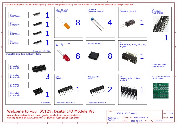
My kits are supplied with a contents sheet which provides a visual guide of the parts included in the kit.
Example kits contents sheet
Some common components are described below. The images shown are typical for the component but they do vary is appearance.
Printed Circuit Board (PCB)
Printed circuit boards come in a range of colours, shapes, and sizes.
Components that have leads passing through the circuit board are called through hole components. Those that do not are called surface mount components.
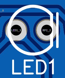
The area surrounding a component hole is called a pad. The ‘lines’ between the holes are called tracks or traces.
Before you start assembly ensure you have correctly identified which side of the PCB the components should be on. This is called the component side. The other side is called the solder side.
Resistors
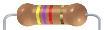
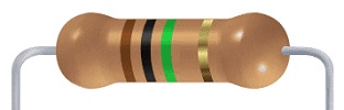
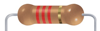
Resistors typically have their resistance (in Ohms) and tolerance (in percent) coded with coloured bands.
The legs will usually need to be bent as shown before insertion into the PCB. Try to bend the legs to exactly match the hole spacing and fit them so they lay nice and flat against the PCB.
Resistors can be fitted either way around as they are not polarity dependent, but they look nicer if the are all the same way around.
Ceramic Capacitors
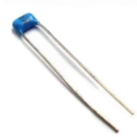
Ceramic capacitors have their capacitance (usually in Pico-Farads) coded numerically, such as “102” for 1000 pF.
The components are usually chosen with leg spacing matching the holes in the PCB.
Ceramic capacitors can be fitted either way around as they are not polarity dependent
Electrolytic Capacitors
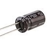
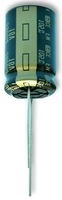
Electrolytic capacitors have their capacitance (usually in Micro-Farads) written on them, such as “100 µF”.
The components are usually chosen with leg spacing matching the holes in the PCB.
Electrolytic capacitors must be fitted the correct way around as they are polarity dependent. The negative lead is usually shorter than the positive lead and is normally indicated with a negative sign. The correct orientation should be indicated on the PCB.
Light Emitting Diodes (LEDs)
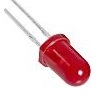
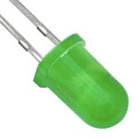
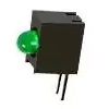
LEDs do not carry any markings for identification, but variations such as light intensity are usually not critical. The colour is usually obvious.
The components are usually chosen with leg spacing matching the holes in the PCB.
LEDs must be fitted the correct way around as they are polarity dependent. The negative lead (Cathode) is usually shorter than the positive lead (Anode). The negative lead is also often indicated by a small flat surface on the side of the LED. The correct orientation should be indicated on the PCB with the negative side shown with a flat and/or straight line.
Sometimes it is desirable to bend the leads so the LED points in the desired direction. In some cases the LED is supplied in a housing to angle it to 90 degrees.
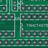
Integrated Circuits (ICs)

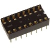
ICs come in a range of sizes and shapes. For retro computers the most common is Dual-In-Line, as illustrated.
ICs are often fitted in sockets rather than being directly soldered to the PCB.
ICs must be fitted the correct way around. Orientation is usually indicated by a notch on the IC and also on the socket. The socket and IC should be fitted such that the notch matches the semi-circle shown on the PCB.
ICs need to be handled with care, as described below.
Handling ICs
When handling ICs you should take precautions to avoid the components being damaged by static electricity. Ideally, this should be an ESD workstation, typically an antistatic mat and wrist strap.
Dual in line components are usually supplied with their legs slightly bent outwards. Before insertion, the legs should be squash together slightly so they are the correct spaced for the socket or PCB.
To avoid bending legs when inserting dual in line ICs into sockets it is best to just press the IC into the socket far enough that it doesn’t fall out, then look between the IC and the socket to check all the legs are lined up correctly before pressing fully down.
Soldering
There are plenty of good soldering guides on the internet, such as:
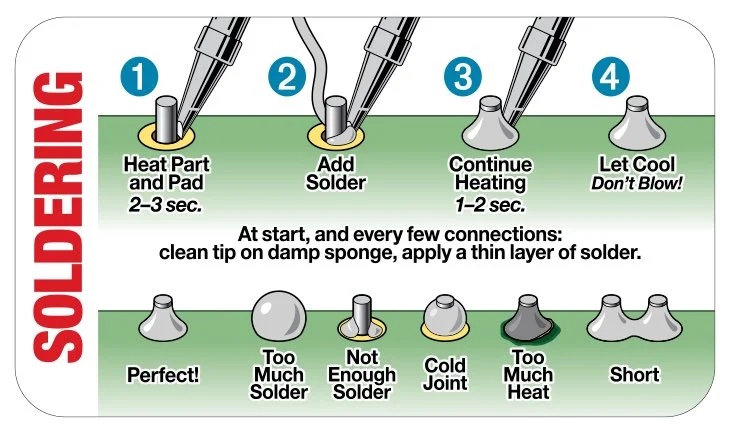
When soldering components with lots of legs, start be soldering just two pins at opposite corners or opposite ends of the component. Then check the component is sitting flat against the PCB. If necessary, adjust by heating the relevant solder joint whilst pressing the component gently against the PCB. Take care not to touch any metal part that is being heated. In the case of long thin components, it is best to solder another pin in the middle and check the component again. When the whole component is flat against the PCB, solder the remaining pins.
Assembly Order
It is generally recommended that smaller components be fitted first. However, I would add a few refinements to that simple strategy. For example, I prefer to leave delicate components until later.
Start by soldering small components that lay flat against the PCB, such as resistors. Bend the leads as required, insert the component through the PCB, then slightly bend the leads on the solder side of the PCB so the component does not fall out when the PCB is turned over. Solder one leg then check the component is still flat against the PCB before soldering the other leg.
By starting with the small components you can lay the board on the worksurface and that will help hold the component against the board as you solder. Some people clamp the PCB in a jig in which case using the worksurface in this way does not apply.
The worksurface strategy works by fitting low profile components first and gradually working up to the taller ones. With this strategy “small components” means low profile components.
After the resistors I usually solder the robust components, such as IC sockets and connectors, starting with the lowest profile components. I generally fit capacitors next and then other components, such as LEDs. Finally, I insert ICs into their sockets.
Testing
Before testing visually inspect everything. I can’t stress this enough. Check all components are in the correct place and in the correct orientation. Check there are no bent IC legs – it is easy to bend an IC leg under the device when inserting into a socket. Check every solder joint is soldering and looks like a good joint. Solder joints should be shiny not dull.
Now inspect it again. Seriously!
Finally, test the board works.
