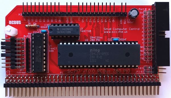
SC717 is a digital I/O module using a Z80 PIO.
- SC717 – Assembly guide
- SC716 – Compatibility
- SC717 – Parts list
- SC717 – Printed circuit board
- SC717 – User guide
- SC700 series information
- SC700 series support
Downloads
- SC717, v1.0, Kit contents sheet (PDF)
- SC717, v1.0, Schematic (PDF)
- SC717, v1.0, PCB design files (OSHWLab)
- SC717, v1.0, Gerber files (ZIP)
Errata
- PCB SC717 v1.0.0 has header pins JP2/3 very tight against the box header P2 so it is best to file a little off the plastic of JP2/3 before soldering it in place
Suppliers
| Kits | Website | From | Currency |
| Small Computers Direct | SCDirect | UK | GBP |
| Stephen C Cousins | Tindie | UK | USD |
| Small Computer Central | Lectronz | UK | Euro/USD |
| PCBs | Website | From | Currency |
| Small Computers Direct | SCDirect | UK | GBP |
| Stephen C Cousins | Tindie | UK | USD |
| Small Computer Central | Lectronz | UK | Euro/USD |
| Assembled and Tested | Website | From | Currency |
| Not available | |||
| Components | |||
| See parts list |
Tindie does not collect VAT for EU countries
Lectronz does collect EU VAT for orders up to 150 EUR
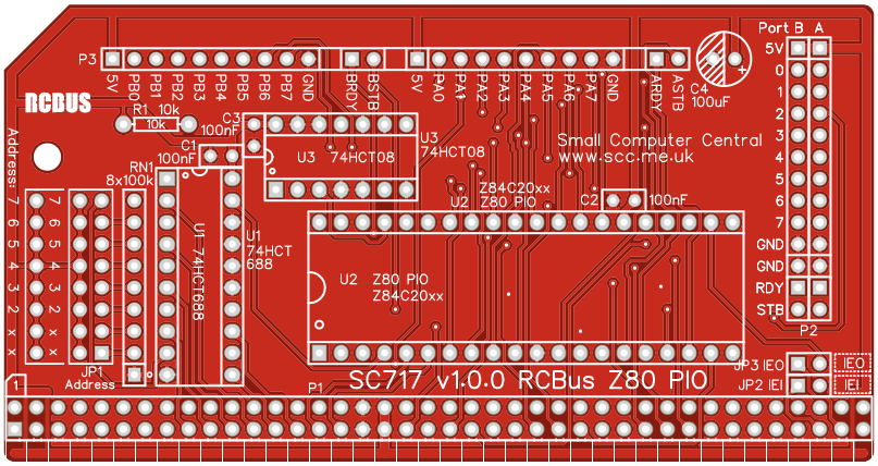
Parts List
| Reference | Qty | Component |
| PCB | 1 | SC717, v1.0, PCB |
| C1 to C3 | 3 | Capacitor, ceramic, 100 nF |
| C4 | 1 | Capacitor, electrolytic, 100 µF |
| JP1 | 1 | Header, male, 2 row x 8 pin, angled |
| JP2 + JP3 | 1 | Header, male, 2 row x 2 pin, angled |
| Jumper | 8 | Jumper shunt |
| P1 | 1 | Header, male, 2 row x 40 pin, angled |
| P2 | 1 | Box header, 2 x 13 pin, angled, or Header, male, 2 x 13 pin, angled |
| P3 | 1 | Header, male, 1 row x 27 pin, angled |
| R1 | 1 | Resistor, 10k, 0.25W |
| RN1 | 1 | Resistor network, 8x100k, SIL, 9-pin |
| Screw (for spacer) | 1 | Machine screw, 6mm, M3 |
| Spacer | 1 | Spacer, 10mm, M3, nylon |
| U1 | 1 | 74HCT688 |
| U2 | 1 | Z80 PIO Z84C2008, or Z80 PIO Z84C2010 |
| U3 | 1 | 74HCT08 |
| IC socket 20-pin U1 | 1 | Socket, DIP, 20-pin |
| IC socket 40-pin U2 | 1 | Socket, DIP, 40 pin |
| IC socket 14-pin U3 | 1 | Socket, DIP, 14-pin |
Printed Circuit Board
User Guide
SC717 is a digital I/O module using a Z80 parallel I/O chip (Z80 PIO) which has 16 general purpose I/O pins plus 4 handshaking pins.
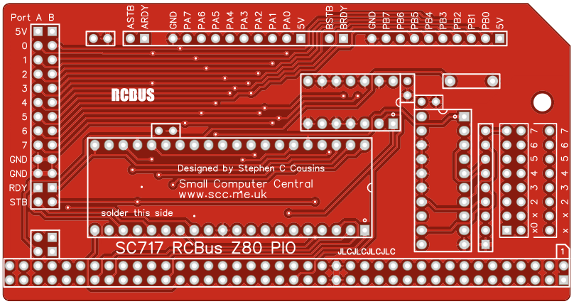
The device address is set with jumpers. All of the I/O pins are available on header pins on the top edge of the PCB and also on a header on the back edge of the PCB.
The module supports the Z80 interrupt priority chain with jumpers to allow it to use the bus pins specified in the RCBus specification. Alternatively, the IEI and IEO signals are available on JP2 and JP3.
Details about programming a Z80 PIO can be found in the Z80 PIO datasheet (PDF).
Example application: Alphanumeric LED (4-bit parallel)
Input/output port functions
| I/O Address | Read | Write |
| Configurable *1 base address | Read Z80 PIO | Write Z80 PIO |
| base + 0 | Port A data | Port A data |
| base + 1 | Port B data | Port B data |
| base + 2 | Port A control | Port A control |
| base + 3 | Port B control | Port B control |
- The RCBus I/O base address should be set to match the software you are using. Typically, this is 0x68 (binary 0110 1000).
Jumper options
| Jumper | Function |
| JP1 | Set module’s RCBus I/O base address The suggested address is 0x68 (binary 0110 1000) |
| JP2 | Connects bus IEI signal to PIO IEI signal The default is jumper shunt not fitted |
| JP3 | Connects bus IEO signal to PIO IEO signal The default is jumper shunt not fitted |
Assembly Guide
Below is the suggested order of assembly. A general guide to assembling circuit boards can be found here.
- Resistors R1
These can be fitted either way around - Header pins P3
Remove pins 11, 14 and 25 to match the holes in the PCB. Pull the pins out of the plastic with pliers, supporting the plastic so as not to break it.. - Decoupling capacitors C1 to C3
These can be fitted either way around - Sockets for U1 to U3
Fit such that the notch in the socket matches the curve in the outline on the PCB silkscreen - Resistor network RN1
This must be fitted the correct way around whereby the dot on the component matches the dot on the PCB silkscreen - Bus header P1
Make sure the pins are parallel to the PCB so that the board is vertical when it is fitted into a backplane socket - Header pins JP1
- Header pins JP2 plus JP3
This is very tight against the box header P2 so it is best to file a little off the plastic of JP2/3 before soldering it in place - Capacitor C4
This must be fitted the correct way around, as described here - Box header or header pins P2
- Insert the integrated circuits into their sockets
Make sure the notch in the component is at the end indicated by the notch in the socket and the curve on the PCB silkscreen - Fit the nylon spacer in the mounting hole
Fit jumper shunts in the positions shown below. All other jumpers are optional and should only be fitted if the feature is required.

Compatibility
This module conforms to the RCBus specification v1.0 for RCBus-2014 and RCBus-Z80.
The RCBus specification includes RCBus-2014 (both RC2014 standard 40-pin bus and RC2014 enhanced 60-pin bus) and also the full 80-pin RCBus. The 80-pin RCBus provides support for advanced Z80 features, such as the interrupt daisy-chain, as well as support for other processor families.
The table below indicates electrical compatibility with each backplane type (40, 60 and 80 pin)

| Backplane | ? | Compatibility notes |
| RCBus 80-pin |  | Fully supported |
| RCBus 60-pin (RC2014 enhanced) | | Limitations: Optional mode 2 interrupt chain requires wires between modules |
| RCBus 40-pin (RC2014 standard) | | Limitations: Optional mode 2 interrupt chain requires wires between modules |
Notes
- This product is designed for hobby use and is not suitable for industrial, commercial, or safety-critical applications.
- The product contains small parts and is not suitable for young children.
