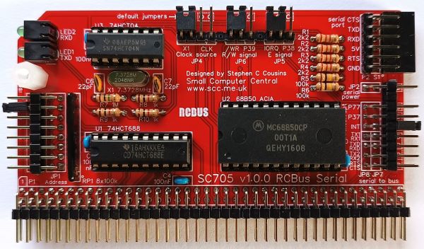
SC705 is a serial port using the 68B50 ACIA with a fixed baud rate of 115200 baud.
- SC705 – Assembly guide
- SC705 – Compatibility
- SC705 – Parts list
- SC705 – Printed circuit board
- SC705 – User guide
- SC700 series information
- SC700 series support
Downloads
- SC705, v1.0, Kit contents sheet (PDF)
- SC705, v1.0, Schematic (PDF)
- SC705, v1.0, PCB design files (OSHWLab)
- SC705, v1.0, Gerber files (ZIP)
Errata
Nothing known
Suppliers
| Kits | Website | From | Currency |
| Small Computers Direct | SCDirect | UK | GBP |
| Stephen C Cousins | Tindie | UK | USD |
| Small Computer Central | Lectronz | UK | Euro/USD |
| PCBs | Website | From | Currency |
| Small Computers Direct | SCDirect | UK | GBP |
| Stephen C Cousins | Tindie | UK | USD |
| Small Computer Central | Lectronz | UK | Euro/USD |
| Assembled and Tested | Website | From | Currency |
| Not available | |||
| Components | |||
| See parts list |
Tindie does not collect VAT for EU countries
Lectronz does collect EU VAT for orders up to 150 EUR
Parts List
| Reference | Qty | Component |
| PCB | 1 | SC705, v1.0, PCB |
| C1 to C4 | 4 | Capacitor, ceramic, 100 nF |
| C5 | 0 | There is no C5 |
| C6 and C7 | 2 | Capacitor, ceramic, 22 pF |
| JP1 | 1 | Header, male, 2 row x 8 pin, angled |
| JP2+3+7+8 | 1 | Header, male, 2 row x 9 pin, angled |
| J4+5+6 | 1 | Header, male, 1 row x 12 pin, angled |
| Jumper | 18 | Jumper shunt |
| LED1 and 2 | 2 | LED, green, 3mm, angled |
| P1 | 1 | Header, male, 2 row x 40 pin, angled |
| P2 | 1 | Header, male, 1 row x 6 pin, angled |
| R1 to R4 | 4 | Resistor, 2k2, 0.25W |
| R5 and R6 | 2 | Resistor, 100k, 0.25W |
| R7 | 1 | Resistor, 1M, 0.25W |
| R8 to R10 | 3 | Resistor, 1k, 0.25W |
| RP1 | 1 | Resistor network, 8x100k, SIL, 9-pin |
| S1 | 1 | Header, female, 1 row x 6 pin, angled |
| Screw (for spacer) | 1 | Machine screw, 6mm, M3 |
| Spacer | 1 | Spacer, 10mm, M3, nylon |
| U1 | 1 | 74HCT688 |
| U2 | 1 | 68B50 ACIA |
| U3 | 1 | 74HCT04 |
| X1 | 1 | Crystal, 7.3728 MHz |
| IC socket 20-pin U1 | 1 | Socket, DIP, 20-pin |
| IC socket 24-pin U2 | 1 | Socket, DIP, 24-pin |
| IC socket 14-pin U3 | 1 | Socket, DIP, 14-pin |
Printed Circuit Board

Note: The PCB is designed to allow a DIP switch to be fitted instead of the header pins JP1.
User Guide
The serial port provides bidirectional asynchronous serial communications usually at 115200 baud, 8 data bits, 1 stop bit, no parity. RTS/CTS handshaking provides hardware flow control in both directions. The interface is at 5-volt (TTL) levels.
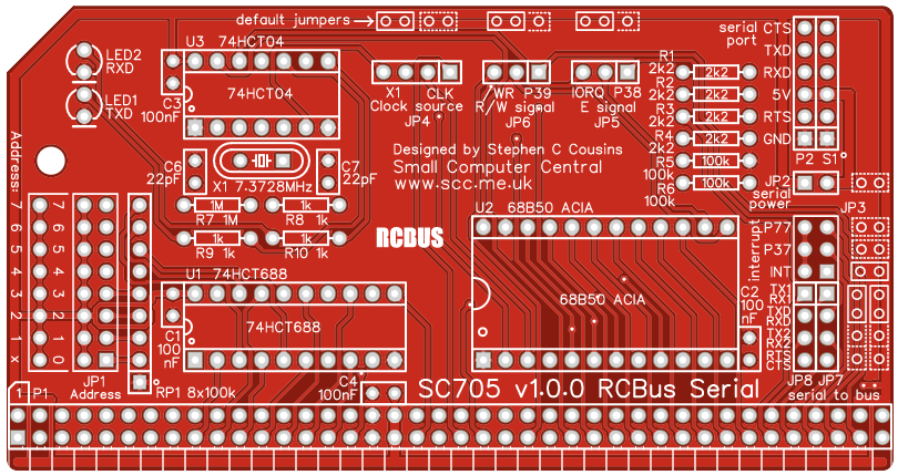
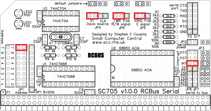
The RCBus I/O port address for this module is set in binary with JP1. Fit a jumper shunt to each bit position where the address bit should be a logic ‘1’ (high voltage).
The default address is 128 decimal, which is 0x80 in hexadecimal and 1000000 in binary. To set this as the address requires a jumper shunt in bit position 8, as illustrated below.
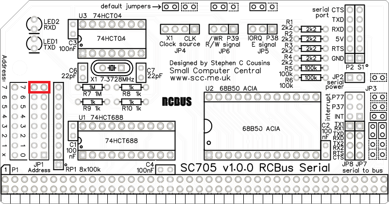
The module occupies two addresses so bit zero of the address can be in either state. The address jumper bit zero is labelled ‘x’ to indicate this.
Jumper JP2 connects the module’s 5-volt supply to the serial port. A jumper should should be fitted here if the RCBus system is being powered from this serial port or if the device connected to this serial port needs to be powered from the RCBus system.
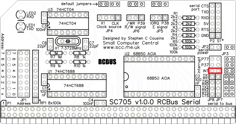
Jumper JP3 enables the ACIA’s interrupt output to be connected to the INT, INT1 or INT2 bus signals. The default position is INT.
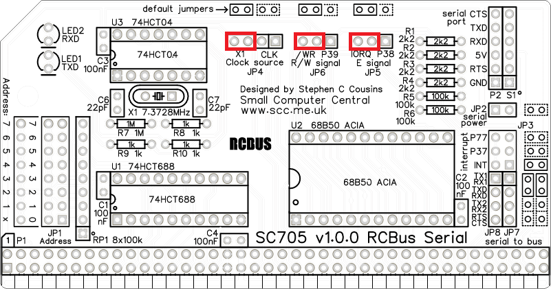
Jumper JP4 enables selection of the clock source for the ACIA. This can either be the on-board 7.3728 MHz oscillator or the RCBus clock signal (CLK). Selecting the on-board clock means the serial port baud rate is independent of the processor speed.
JP5 and JP6 enable selection of the ACIA’s R/W and E inputs. Normally these are set to the IORQ and WR signals that are common to all implementations of the RCBus. Alternative, if the processor supports native R/W and E signals then these can be selected instead.
JP7 and JP8 enable the ACIA’s RXD and TXD signals to be connected to the RCBus RX and TX pins, and the ACIA’s CTS and RTS signals to be connected to the RCBus RX2 and TX2 pins. To connect all of these signals, fit jumper shunts in the positions illustrated below.
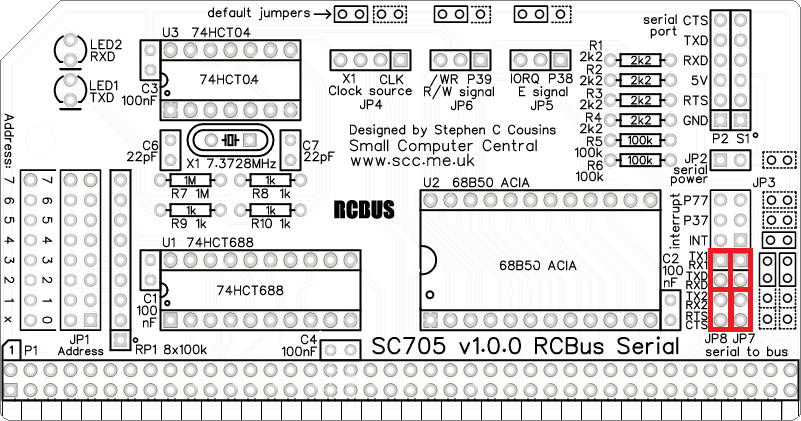
It is also possible to connect the ACIA’s RXD and TXD signals to the RCBus RX2 and TX2 pins. This is achieved by fitting one pair of jumper shunts in the middle positions, as illustrated below.

Input/output port functions
| RCBus I/O Address | Read | Write |
| Configurable *1 | 0x80 | 0x80 |
- The RCBus I/O address should be set to match the software you are using. Typically, this is 0x80 or 0x40.
Jumper options
| Jumper | Function |
| JP 1 | Set SC705’s RCBus I/O address |
| JP 2 | Connects 5-volt power to serial port |
| JP 3 | Selects which interrupt signal is generated JP 3.1 Interrupt goes to RCBus INT signal JP 3.2 Interrupt goes to RCBus INT1 signal JP 3.3 Interrupt goes to RCBus INT2 signal The default is INT |
| JP 4 | Select the clock source JP 4.1-2 Clock source is the RCBus CLOCK signal JP 4.3-4 On-board 7.2728 MHz oscillator If jumper shunts are fitted in both positions the on-board oscillator supplies the RCBus CLOCK signal The default is the on-board oscillator |
| JP 5 | Select the E signal source JP 5.1-2 RCBus pin 38 (for use with 68xx processors) JP 5.2-3 RCBus nIORQ (inverted) The default is the inverted nIORQ signal |
| JP 6 | Selects to R/W signal source JP 6.1-2 RCBus pin 39 (for use with 68xx processors) JP 6.2-3 RCBus nWR signal The default is the nWR signal |
| JP 7 | Connects the RXD input and the CTS input to the bus JP 7.1-2 Connects RXD to bus RX(1) signal JP 7.3-4 Connects CTS to bus RX2 signal |
| JP 8 | Connects the TXD output and the RTS output to the bus JP 8.1-2 Connects TXD to bus TX(1) signal JP 8.3-4 Connects RTS to bus TX2 signal |
Assembly Guide
Below is the suggested order of assembly. A general guide to assembling circuit boards can be found here.
- Resistors R1 to R10
- Socket S1
- Decoupling capacitors C1 to C5
These can be fitted either way around - Resistor network RP1
- IC sockets for U1 to U3
Ensure the notch in the socket matches the marking on the PCB - Capacitors C6 and C7
- Header pins JP4, JP5 and JP6
Fit as one strip with pins 4 and 8 removed - Header pins P2
- Header pins JP1
You may wish to remove the pins for address bit zero as the module occupies two I/O addresses and therefore bit zero is not used - Header pins JP2, JP3, JP7 and JP8
Fit as one strip with pins 2 removed - Bus header pins P1
- LED1 and LED2
The angled LEDs in the kit only fit one way around, but standard LEDs need to have the short lead in the hole marked with a flat line - Crystal X1
- Fit the IC’s in their sockets
Ensure the notch in the IC matches the PCB and IC socket - Fit jumper shunts in the default positions (see below)
- Fit the nylon spacer in the mounting hole
Compatibility
This module conforms to the RCBus specification v1.0 for RCBus-2014, RCBus-Z80 and RCBus-68xx.
The RCBus specification includes RCBus-2014 (both RC2014 standard 40-pin bus and RC2014 enhanced 60-pin bus) and also the full 80-pin RCBus. The 80-pin RCBus provides support for advanced Z80 features, such as the interrupt daisy-chain, as well as support for other processor families.
The table below indicates electrical compatibility with each backplane type (40, 60 and 80 pin)

| Backplane | ? | Compatibility notes |
| RCBus 80-pin |  | Fully supported |
| RCBus 60-pin (RC2014 enhanced) | | Fully supported |
| RCBus 40-pin (RC2014 standard) | | Limitations: Some optional signals are not available (TX2, RX2) |
The following table indicates electrical compatibility with SC705. Check firmware and software details for any required software support.
| Product (80-pin) | ? | Compatibility notes |
| SC126 Z180 motherboard | | Adds Z180 SBC/ motherboard |
| SC701 Backplane 6+1 | | Adds 6 module sockets RCBus 80-pin and PSU |
| SC702 Backplane 6+1 | | Adds 6 module sockets RCBus 80-pin |
| SC703 Power from 12v | | Adds power supply (8 to 12 volt input) and reset |
| SC704 I2C bus master | | Adds I2C bus master |
| SC705 Serial ACIA | | Can add more than one Serial ACIA module |
| SC706 Z80 CPU | | Adds Z80 CPU and main bus clock |
| SC707 Memory 128k | | Adds 128k RAM and 128k flash ROM |
| SC708 Z80 SBC | | Adds CPU, ROM, RAM clock and reset |
| SC709 Backplane 12+1 | | Adds 12 module sockets RCBus 80-pin and PSU |
| SC710 Backplane 12+1 | | Adds 12 module sockets RCBus 80-pin |
| SC711 Prototyping | | Prototyping module |
| SC712 Power from 5v | | Adds power supply (5 volt input) and reset |
| SC713 RCBus tool | n/a | Simple reference tool No electrical function |
| SC714 Memory 512k | | Adds 512k RAM and 512k flash ROM |
| SC715 Compact flash | | Adds Compact Flash storage |
| SC716 Z80 SIO/2 | | Adds two serial ports Typically set to 0x84 |
| SC717 Z80 PIO | | Adds parallel I/O using Z80 PIO |
| SC718 Z80 CTC | | Adds counter/timer using Z80 CTC |
| SC719 Digital I/O | | Adds digital I/O Eight in, eight out |
| SC720 Z80 motherboard | | Adds Z80 SBC/ motherboard |
| SC721 Memory 512k | | Adds 512k RAM and 2 x 512k flash ROM |
| SC722 Z180 CPU | | Adds Z180 CPU with two serial ports |
| SC723 Backplane 3 | | Adds 3 module sockets RCBus 80-pin |
| SC724 Breakout | | Prototyping breakout module |
| SC725 SIO+CTC | | Adds two serial ports and 4 counter/timers |
| SC726 Clock generator | | Generates CLK and CLK2 bus signals |
| SC727 Real time clock | | Adds real time clock for time and date |
| SC728 Module riser | | Simple module riser for RCBus 80-pin |
| SC791 Z80 system | | Modular Z80 system |
| SC792 Z180 system | | Modular Z180 system |
| Product (40 pin) | ? | Compatibility notes |
| SC114 Z80 motherboard | | Adds Z80 SBC/ motherboard |
| SC130 Z180 motherboard | | Adds Z180 SBC/ motherboard |
| SC133 Backplane 11+1 | | Adds 11 module sockets RCBus 40-pin and PSU |
| SC134 LED output port | | Adds eight LED outputs |
| SC135 Digital output port | | Adds eight digital outputs |
| SC136 Digital input port | | Adds eight digital inputs |
| SC137 I2C bus master | | Adds I2C bus master |
| SC139 Serial ACIA | | Can add more than one Serial ACIA module |
| SC141 Backplane 12+1 | | Adds 12 module sockets RCBus 40-pin |
| SC142 Power from 12v | | Adds power supply (8 to 12 volt input) and reset |
| SC143 Flash ROM | | Adds 128k flash ROM |
| SC145 Compact flash | | Adds Compact Flash storage |
| SC147 Backplane 6+1 | | Adds 6 module sockets RCBus 40-pin |
| SC148 Power from 5v | | Adds power supply (5 volt input) and reset |
| SC149 Z80 CPU | | Adds Z80 CPU and main bus clock |
| SC150 Paged RAM 128k | | Adds 128k of paged RAM |
| SC151 Paged ROM 128k | | Adds 128k of paged ROM |
| Other suppliers | ? | Compatibility notes |
| RC2014 Mini system | | Adds Z80 SBC/ motherboard |
| RC2014 Pro system | | Modular Z80 system |
| RC2014 Zed system | | Modular Z80 system |
| RC2014 Micro module | | Adds CPU, ROM, RAM serial, clock and reset |
| RC2014 Backplane 5 | | Adds 5 module sockets RC2014 40-pin |
| RC2014 Backplane 8 | | Adds 12 module sockets RC2014 40-pin |
| RC2014 Backplane Pro | | Adds 12 module sockets RC2014 40-pin / 60-pin |
| RC2014 Z80 CPU | | Adds Z80 CPU |
| RC2014 SIO/2 dual serial | | Adds two serial ports at 0x80 to 0x87 |
| RC2014 Compact flash | | Adds Compact Flash at 0x10 to 0x17 |
| RC2014 Dual clock | | Generates CLK and CLK2 bus signals |
| RC2014 Pageable ROM | | Adds 64k paged ROM |
| RC2014 64k RAM | | Adds 64k paged RAM |
| RC2014 Memory 512k | | Adds 512k RAM and 512k flash ROM |
| RC2014 Digital I/O | | Adds eight LED outputs and eight push buttons |
| RC2014 Real time clock | | Adds real time clock for time and date |
| RC2014 RP2040 VGA terminal | | Connect VGA monitor and USB keyboard |
| RC2014 Pi Pico terminal | | Connect VGA monitor and USB keyboard |
| RC2014 YM2149 sound card | | Adds authentic retro sound |
| Weird electronics Flock v2 | | Adds floppy disk and real time clock |
Notes
- This product is designed for hobby use and is not suitable for industrial, commercial, or safety-critical applications.
- The product contains small parts and is not suitable for young children.
