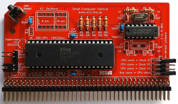
SC706 is a Z80 Central Processor Unit (CPU) module with three clock oscillator options, and an optional voltage supervisor and reset device, designed for the RCBus.
- SC706 – Assembly guide
- SC706 – Compatibility
- SC706 – Parts list
- SC706 – Printed circuit board
- SC706 – User guide
- SC700 series information
- SC700 series support
Downloads
- SC706, v1.0, Kit contents sheet (PDF)
- SC706, v1.0, Schematic (PDF)
- SC706, v1.0, PCB design files (OSHWLab)
- SC706, v1.0, Gerber files (ZIP)
Errata
- PCB SC706 v1.0.0 needs a wire link for capacitor C7 if the oscillator X2 is not populated
Suppliers
| Kits | Website | From | Currency |
| Small Computers Direct | SCDirect | UK | GBP |
| Stephen C Cousins | Tindie | UK | USD |
| Small Computer Central | Lectronz | UK | Euro/USD |
| PCBs | Website | From | Currency |
| Small Computers Direct | SCDirect | UK | GBP |
| Stephen C Cousins | Tindie | UK | USD |
| Small Computer Central | Lectronz | UK | Euro/USD |
| Assembled and Tested | Website | From | Currency |
| Not available | |||
| Components | |||
| See parts list |
Tindie does not collect VAT for EU countries
Lectronz does collect EU VAT for orders up to 150 EUR
Parts List
| Reference | Qty | Component |
| PCB | 1 | SC706, v1.0, PCB |
| C1 to C4 | 4 | Capacitor, ceramic, 100 nF |
| C5 and C6 | 2 | Capacitor, ceramic, 22 pF |
| C7 and C8 | 0 | Capacitor, ceramic, ~22 pF Not included in the kit Fit a wire link at C7 |
| C9 | 1 | Capacitor, ceramic, 1 nF Not included in the kit |
| JP1 | 1 | Header, male, 2 row x 4 pin, angled or male, 2 row x 4 pin, straight Angled pins included in kit |
| JP2 | 1 | Header, male, 1 row x 2 pin, angled or male, 1 row x 2 pin, straight Angled pins included in kit |
| Jumper | 2 | Jumper shunt |
| P1 | 1 | Header, male, 2 row x 40 pin, angled |
| P2 | 1 | Header, male, 1 row x 2 pin, angled or male, 1 row x 2 pin, straight Angled pins included in kit |
| R1 | 1 | Resistor, 1M, 0.25W |
| R2 | 1 | Resistor, 1k, 0.25W |
| R3 | 0 | Resistor, ~1M, 0.25W Not included in the kit |
| R4 | 0 | Resistor, ~1k, 0.25W Not included in the kit |
| R5 to R9 | 5 | Resistor, 10k, 0.25W |
| SW1 | 1 | Switch, tactile button, angled |
| Screw (for spacer) | 1 | Machine screw, 6mm, M3 |
| Spacer | 1 | Spacer, 10mm, M3, nylon |
| U1 | 1 | Z80 CPU, Z84C0008PEG, or Z80 CPU, Z84C0010PEG |
| U2 | 1 | 74HCT04 |
| U3 | 1 | DS1233-5+ supervisor Not included in the kit |
| X1 | 1 | Crystal, 7.3728MHz |
| X2 | 0 | Crystal, typically 2 to 10MHz Not included in the kit |
| X3 | 0 | Oscillator, 8 or 14-pin Not included in the kit |
| IC socket 40-pin U1 | 1 | Socket, DIP, 40 pin |
| IC socket 14-pin U2 | 1 | Socket, DIP, 14-pin |
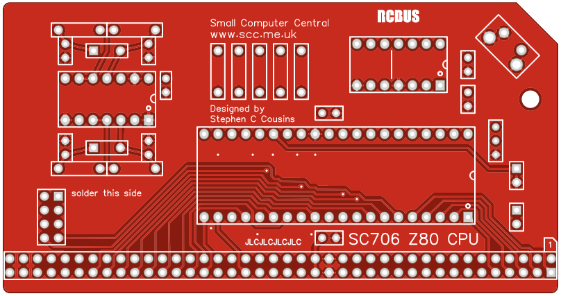
Printed Circuit Board

User Guide
This module conforms to the RCBus specification v1.0 for RCBus-2014 and RCBus-Z80.
SC706 provides a Z80 Central Processor Unit (CPU) module with three clock oscillator options, and an optional voltage supervisor and reset device, designed for the RCBus.
The PCB has three clock oscillators, with the required oscillator selected with a jumper. This allows several different oscillators to be including with easy selection of the desired clock source. The kit includes parts for clock oscillator 1 only (7.3728 MHz). If X2 is not populated, solder a link across C7 so the input to U2 is not left floating. Strange things can happen if it is left floating.
It is also possible to build the PCB without any of the oscillator parts and use a clock source from a different module on the bus. Alternatively, the clock source selection jumper (X1, X2 or X3) can be left off so the onboard oscillator(s) are isolated and not used. This jumper simply connects the required oscillator output to the CPU’s clock input pin.
There is also a jumper to allow the CPU’s clock to be connected to the RCBus CLK signal. This is normally desirable but it can be isolated if required.
If fitted, the voltage supervisor and reset device (U3) provides a reliable power up reset. It works by holding the CPU in reset until the supply voltage reaches approximately 4.75 volts. If the system does not seem to be working, always check the supply voltage is above 4.75 volts on the PCB and that the RESET signal is a logic high voltage, typically above 4 volts. The supervisor should hold the reset low of about 0.5 seconds after the system is turned on and after the reset button is released.
The system should only include one enabled voltage supervisor, so a jumper option has been provided to connect or isolate this device. Normally, it should be connected, but if you have a supervisor on another module you may need to isolate this one.
Input/output port functions
| I/O Address | Read | Write |
| none | n/a | n/a |
Jumper options
| Jumper | Function |
| JP 1 | Clock signals JP1.1 connects CPU clock to Clock X1 JP1.2 connects CPU clock to Clock X2 JP1.3 connects CPU clock to Clock X3 JP1.4 connects Bus clock to CPU clock |
| JP 2 | Enable voltage supervisor |
Clock oscillators X2 and X3 are optional. The default is to connect the output of clock oscillator X1 to the CPU and the RCBus CLK pin. This requires a jumper shunt in each of the two marked default positions (JP1.1 and JP1.4). If you wish to use a clock sourced from a different module then the X1 jumper should be removed.
Fit a jumper shunt to JP2 if the voltage supervisor is to be used. This jumper connects the voltage supervisor to the RESET signal. The system should only contain one enabled supervisor, thus the jumper has been provided to isolate or connect this device.
Assembly Guide
Below is the suggested order of assembly. A general guide to assembling circuit boards can be found here.
The kit does not include parts for the optional oscillators X2 and X3. Fit a wire link for capacitor C7 if the oscillator X2 is not populated.
- Resistors R1, R2, R5, R6, R7, R8 and R9
These can be fitted either way around - Decoupling capacitors C1, C2, C3 and C4
These can be fitted either way around - Header pins JP2 and P2
This can be a single strip of 5 pins with the middle pin removed - Sockets for U1 and U2
Fit such that the notch in the socket matches the curve in the outline on the PCB silkscreen - Capacitors C5 and C6
These can be fitted either way around - If X2 is not going to be populated, solder a link across C7 so the input to U2 is not left floating. Strange things can happen if it is left floating
- Bus header P1
Make sure the pins are parallel to the PCB so that the board is vertical when it is fitted into a backplane socket - Header pins JP1
- Crystal X1
This can be fitted either way around - Switch SW1
- Fit a jumper shunts in the default “CPU clock = Clock X1” and “Bus clock = CPU clock” positions of JP1, as indicated on the PCB
- Fit a jumper shunt to JP2 only if you want the voltage supervisor on this board to be enabled. You should only have one voltage supervisor enabled in your system.
- Insert the integrated circuits into their sockets
Make sure the notch in the component is at the end indicated by the notch in the socket and the curve on the PCB silkscreen - Fit the nylon spacer in the mounting hole
Compatibility
This module conforms to the RCBus specification v1.0 for RCBus-2014 and RCBus-Z80.
The RCBus specification includes RCBus-2014 (both RC2014 standard 40-pin bus and RC2014 enhanced 60-pin bus) and also the full 80-pin RCBus. The 80-pin RCBus provides support for advanced Z80 features, such as the interrupt daisy-chain, as well as support for other processor families.
The table below indicates electrical compatibility with each backplane type (40, 60 and 80 pin)

| Backplane | ? | Compatibility notes |
| RCBus 80-pin |  | Fully supported |
| RCBus 60-pin (RC2014 enhanced) | | Fully supported |
| RCBus 40-pin (RC2014 standard) | | Limitations: Some optional signals are not available (/NMI, /WAIT, /RFSH, /HALT, /BUSAK, /BUSRQ) |
The following table indicates electrical compatibility with SC706. Check firmware and software details for any required software support.
| Product (80-pin) | ? | Compatibility notes |
| SC126 Z180 motherboard |  | Function conflict |
| SC701 Backplane 6+1 | | Adds 6 module sockets RCBus 80-pin and PSU |
| SC702 Backplane 6+1 | | Adds 6 module sockets RCBus 80-pin |
| SC703 Power from 12v | | Adds power supply (8 to 12 volt input) and reset |
| SC704 I2C bus master | | Adds I2C bus master |
| SC705 Serial ACIA | | Adds one serial port Typically set to 0x40 |
| SC706 Z80 CPU | | Function conflict |
| SC707 Memory 128k | | Adds 128k RAM and 128k flash ROM |
| SC708 Z80 SBC | | Function conflict |
| SC709 Backplane 12+1 | | Adds 12 module sockets RCBus 80-pin and PSU |
| SC710 Backplane 12+1 | | Adds 12 module sockets RCBus 80-pin |
| SC711 Prototyping | | Prototyping module |
| SC712 Power from 5v | | Adds power supply (5 volt input) and reset |
| SC713 RCBus tool | n/a | Simple reference tool No electrical function |
| SC714 Memory 512k | | Adds 512k RAM and 512k flash ROM |
| SC715 Compact flash | | Adds Compact Flash storage |
| SC716 Z80 SIO/2 | | Adds two serial ports Typically set to 0x84 |
| SC717 Z80 PIO | | Adds parallel I/O using Z80 PIO |
| SC718 Z80 CTC | | Adds counter/timer using Z80 CTC |
| SC719 Digital I/O | | Adds digital I/O Eight in, eight out |
| SC720 Z80 motherboard | | Function conflict |
| SC721 Memory 512k | | Needs a memory management unit |
| SC722 Z180 CPU | | Function conflict |
| SC723 Backplane 3 | | Adds 3 module sockets RCBus 80-pin |
| SC724 Breakout | | Prototyping breakout module |
| SC725 SIO+CTC | | Adds two serial ports and 4 counter/timers |
| SC726 Clock generator | | Generates CLK and CLK2 bus signals |
| SC727 Real time clock | | Adds real time clock for time and date |
| SC728 Module riser | | Simple module riser for RCBus 80-pin |
| SC791 Z80 system | | Function conflict |
| SC792 Z180 system | | Function conflict |
| Product (40 pin) | ? | Compatibility notes |
| SC114 Z80 motherboard | | Function conflict |
| SC130 Z180 motherboard | | Function conflict |
| SC133 Backplane 11+1 | | Adds 11 module sockets RCBus 40-pin and PSU |
| SC134 LED output port | | Adds eight LED outputs |
| SC135 Digital output port | | Adds eight digital outputs |
| SC136 Digital input port | | Adds eight digital inputs |
| SC137 I2C bus master | | Adds I2C bus master |
| SC139 Serial ACIA | | Adds one serial port Typically set to 0x40 |
| SC141 Backplane 12+1 | | Adds 12 module sockets RCBus 40-pin |
| SC142 Power from 12v | | Adds power supply (8 to 12 volt input) and reset |
| SC143 Flash ROM | | Adds 128k flash ROM |
| SC145 Compact flash | | Adds Compact Flash storage |
| SC147 Backplane 6+1 | | Adds 6 module sockets RCBus 40-pin |
| SC148 Power from 5v | | Adds power supply (5 volt input) and reset |
| SC149 Z80 CPU | | Function conflict |
| SC150 Paged RAM 128k | | Adds 128k of paged RAM |
| SC151 Paged ROM 128k | | Adds 128k of paged ROM |
| Other suppliers | ? | Compatibility notes |
| RC2014 Mini system | | Function conflict |
| RC2014 Pro system | | Function conflict |
| RC2014 Zed system | | Function conflict |
| RC2014 Micro module | | Function conflict |
| RC2014 Backplane 5 | | Adds 5 module sockets RC2014 40-pin |
| RC2014 Backplane 8 | | Adds 12 module sockets RC2014 40-pin |
| RC2014 Backplane Pro | | Adds 12 module sockets RC2014 40-pin / 60-pin |
| RC2014 Z80 CPU | | Function conflict |
| RC2014 SIO/2 dual serial | | Adds two serial ports at 0x80 to 0x87 |
| RC2014 Compact flash | | Adds Compact Flash at 0x10 to 0x17 |
| RC2014 Dual clock | | Generates CLK and CLK2 bus signals |
| RC2014 Pageable ROM | | Adds 64k paged ROM |
| RC2014 64k RAM | | Adds 64k paged RAM |
| RC2014 Memory 512k | | Adds 512k RAM and 512k flash ROM |
| RC2014 Digital I/O | | Adds eight LED outputs and eight push buttons |
| RC2014 Real time clock | | Adds real time clock for time and date |
| RC2014 RP2040 VGA terminal | | Connect VGA monitor and USB keyboard |
| RC2014 Pi Pico terminal | | Connect VGA monitor and USB keyboard |
| RC2014 YM2149 sound card | | Adds authentic retro sound |
| Weird electronics Flock v2 | | Adds floppy disk and real time clock |
Notes
- This product is designed for hobby use and is not suitable for industrial, commercial, or safety-critical applications.
- The product contains small parts and is not suitable for young children.
