SC707 is a memory module with 128k bytes of FLASH ROM and 128k pages of RAM designed for the RCBus. This module provides suitable memory for running CP/M.
- SC707 – Assembly Guide
- SC707 – Compatibility
- SC707 – Firmware (SCM S8)
- SC707 – Parts List
- SC707 – Printed Circuit Board
- SC707 – User Guide
- SC700 series information
- SC700 series support
Downloads
- SC707, v1.0, Kit contents sheet (PDF)
- SC707, v1.0, Schematic (PDF)
- SC707, v1.0, PCB design files (OSHWLab)
- SC707, v1.0, Gerber files (ZIP)
Errata
Nothing known
Suppliers
| Kits | Website | From | Currency |
| Small Computers Direct | SCDirect | UK | GBP |
| Stephen C Cousins | Tindie | UK | USD |
| Small Computer Central | Lectronz | UK | Euro/USD |
| PCBs | Website | From | Currency |
| Small Computers Direct | SCDirect | UK | GBP |
| Stephen C Cousins | Tindie | UK | USD |
| Small Computer Central | Lectronz | UK | Euro/USD |
| Assembled and Tested | Website | From | Currency |
| Not available | |||
| Components | |||
| See parts list |
Tindie does not collect VAT for EU countries
Lectronz does collect EU VAT for orders up to 150 EUR
Parts List
| Reference | Qty | Component |
| PCB | 1 | SC707, v1.0, PCB |
| C1 to C4 | 4 | Capacitor, ceramic, 100 nF |
| JP1+2+3 | 1 | Header, male, 2 row x 10 pin, angled |
| Jumper | 3 | Jumper shunt |
| LED1 and 2 | 2 | LED, green, 3mm, angled |
| P1 | 1 | Header, male, 2 row x 40 pin, angled |
| R1 and R2 | 2 | Resistor, 1k, 0.25W |
| Screw (for spacer) | 1 | Machine screw, 6mm, M3 |
| Spacer | 1 | Spacer, 10mm, M3, nylon |
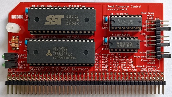
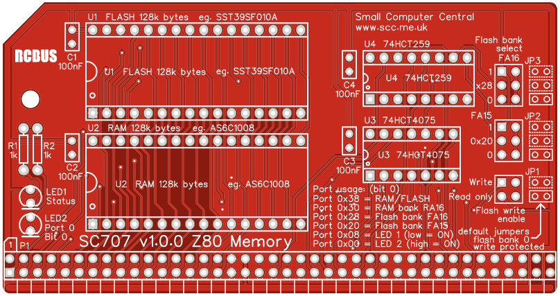
| U1 | 1 | FLASH 128k bytes SST39SF010A |
| U2 | 1 | RAM 128k bytes AS6C1008 |
| U3 | 1 | 74HCT4075 |
| U4 | 1 | 74HCT259 |
| IC socket 32-pin U1 and U2 | 2 | Socket, DIP, 32-pin |
| IC socket 14-pin U3 | 1 | Socket, DIP, 14-pin |
| IC socket 16-pin U4 | 1 | Socket, DIP, 16-pin |
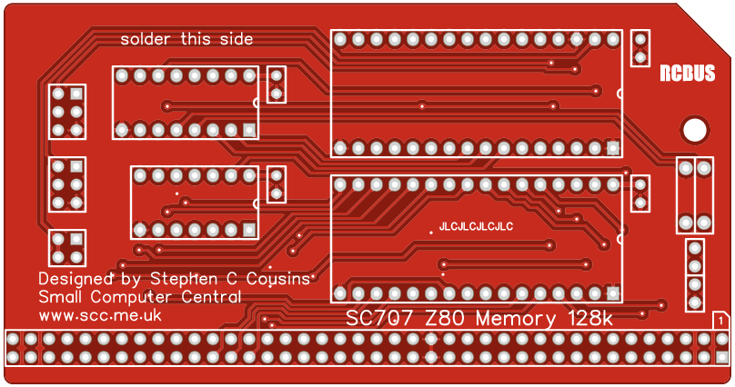
Printed Circuit Board
User Guide
SC707 provides 128k of banked FLASH ROM and 128k bytes of RAM, together with paging control of the lower 32k. This configuration is suitable to run CP/M 2.
At reset the output bits of integrated circuit U4 are all cleared to zero (low voltage). The ROM is paged into memory from 0x0000 to 0x7FFF (32k bytes) with RAM from 0x8000 to 0xFFFF (32k bytes). When input/output address 0x38 bit 0 is set to one (a high voltage) the ROM is paged out and RAM is paged in, giving a full 64k bytes of RAM from 0x0000 to 0xFFFF.
The 128k bytes of FLASH ROM is split into four 32k byte banks. The bank is selected with JP2 (FLASH address A15) and JP3 (FLASH address A16). By default these jumpers should be set to ‘0’ selecting the lowest 32k bytes. By setting jumpers to either 0 or 1, any of the four banks can be selected. Alternatively, these jumpers can be set for software selection of the bank, using output addresses 0x20 bit 0 and 0x28 bit 0.
The 128k bytes of RAM is split into two 64k byte banks. The bank can be selected with output addresses 0x30 bit 0
The status LED should be ON when the system is in reset. With the recommended firmware, the LED should flash OFF for about half a second when the system is released from reset. It should then turn ON and stay on. User software can then control the LED, as required.
Input/output port functions
| I/O Address | Read | Write |
| 0x00 (0x00 to 0x03) | n/a | User LED (LED 2) Low = OFF, high = ON |
| 0x08 (0x08 to 0x0B) | n/a | Status LED (LED 1) Low = ON, high = OFF |
| 0x20 (0x20 to 0x23) | n/a | ROM bank select FA15 |
| 0x28 (0x28 to 0x2B) | n/a | ROM bank select FA16 |
| 0x30 (0x30 to 0x33) | n/a | RAM bank select RA16 |
| 0x38 (0x38 to 0x3B) | n/a | Memory paging (lower 32k) Low = ROM, high = RAM |
Jumper options
| Jumper | Function |
| JP1 | FLASH write enable / protect Read only = Write protected Write = Read and write enabled |
| JP2 | FLASH bank select JP2.1 = FLASH A15 high JP2.2 = Software select FLASH A15 via port 0x20 JP2.3 = FLASH A15 low |
| JP3 | FLASH bank select JP3.1 = FLASH A16 high JP3.2 = Software select FLASH A16 via port 0x28 JP3.3 = FLASH A16 low |
It is recommended that a jumper shunt be fitted in the “Read only” position of JP1 during normal use. It only needs to be in the “Write” position when the contents of the FLASH is to be updated. While the FLASH device requires a very specific sequence of events to protect it against accidental modification, it is best to play safe and use the jumper to ensure it can not be written to.
Assembly Guide
Below is the suggested order of assembly. A general guide to assembling circuit boards can be found here.
- Resistors R1 and R2
These can be fitted either way around - Sockets for U1, U2 and U3
Fit such that the notch in the socket matches the curve in the outline on the PCB silkscreen - Bus header P1
Make sure the pins are parallel to the PCB so that the board is vertical when it is fitted into a backplane socket - Decoupling capacitors C1, C2, C3 and C4
These can be fitted either way around - Light emitting diodes LED1 and LED2
Fit such that the short lead and/or small flat on the plastic is at the end marked with a line on the PCB silkscreen - Header pins JP1, JP2 and JP3
This can be one header with a few pins pulled out or three separate headers. Fit a jumper shunts in the “Read only” position of JP1 and in position “0” of JP2 and JP3 - Insert the integrated circuits into their sockets
Make sure the notch in the component is at the end indicated by the notch in the socket and the curve on the PCB silkscreen - Fit the nylon spacer in the mounting hole
Compatibility
This module conforms to the RCBus specification v1.0 for RCBus-2014 and RCBus-Z80.
The RCBus specification includes RCBus-2014 (both RC2014 standard 40-pin bus and RC2014 enhanced 60-pin bus) and also the full 80-pin RCBus. The 80-pin RCBus provides support for advanced Z80 features, such as the interrupt daisy-chain, as well as support for other processor families.
The table below indicates electrical compatibility with each backplane type (40, 60 and 80 pin)

| Backplane | ? | Compatibility notes |
| RCBus 80-pin |  | Fully supported |
| RCBus 60-pin (RC2014 enhanced) | | Fully supported |
| RCBus 40-pin (RC2014 standard) | | Fully supported |
The following table indicates electrical compatibility with SC707. Check firmware and software details for any required software support.
| Product (80-pin) | ? | Compatibility notes |
| SC126 Z180 motherboard |  | Function conflict |
| SC701 Backplane 6+1 | | Adds 6 module sockets RCBus 80-pin and PSU |
| SC702 Backplane 6+1 | | Adds 6 module sockets RCBus 80-pin |
| SC703 Power from 12v | | Adds power supply (8 to 12 volt input) and reset |
| SC704 I2C bus master | | Adds I2C bus master |
| SC705 Serial ACIA | | Adds one serial port Typically set to 0x40 |
| SC706 Z80 CPU | | Adds Z80 CPU and main bus clock |
| SC707 Memory 128k | | Function conflict |
| SC708 Z80 SBC | | Function conflict |
| SC709 Backplane 12+1 | | Adds 12 module sockets RCBus 80-pin and PSU |
| SC710 Backplane 12+1 | | Adds 12 module sockets RCBus 80-pin |
| SC711 Prototyping | | Prototyping module |
| SC712 Power from 5v | | Adds power supply (5 volt input) and reset |
| SC713 RCBus tool | n/a | Simple reference tool No electrical function |
| SC714 Memory 512k | | Function conflict |
| SC715 Compact flash | | Adds Compact Flash storage |
| SC716 Z80 SIO/2 | | Adds two serial ports Typically set to 0x84 |
| SC717 Z80 PIO | | Adds parallel I/O using Z80 PIO |
| SC718 Z80 CTC | | Adds counter/timer using Z80 CTC |
| SC719 Digital I/O | | Adds digital I/O Eight in, eight out |
| SC720 Z80 motherboard | | Function conflict |
| SC721 Memory 512k | | Function conflict |
| SC722 Z180 CPU | | Adds Z180 CPU with two serial ports |
| SC723 Backplane 3 | | Adds 3 module sockets RCBus 80-pin |
| SC724 Breakout | | Prototyping breakout module |
| SC725 SIO+CTC | | Adds two serial ports and 4 counter/timers |
| SC726 Clock generator | | Generates CLK and CLK2 bus signals |
| SC727 Real time clock | | Adds real time clock for time and date |
| SC728 Module riser | | Simple module riser for RCBus 80-pin |
| SC729 Compact flash | | Adds Compact Flash storage |
| SC730 Z80 CPU + MMU | | Function conflict |
| SC731 Dual PWM | | Adds two PWM outputs |
| SC732 Dual servo | | Adds two servo outputs |
| SC733 Prototyping | | Prototyping module |
| SC791 Z80 system | | Function conflict |
| SC792 Z180 system | | Function conflict |
| SC794 Z80 system | | Function conflict |
| Product (40 pin) | ? | Compatibility notes |
| SC114 Z80 motherboard | | Function conflict |
| SC130 Z180 motherboard | | Function conflict |
| SC133 Backplane 11+1 | | Adds 11 module sockets RCBus 40-pin and PSU |
| SC134 LED output port | | Adds eight LED outputs |
| SC135 Digital output port | | Adds eight digital outputs |
| SC136 Digital input port | | Adds eight digital inputs |
| SC137 I2C bus master | | Adds I2C bus master |
| SC139 Serial ACIA | | Adds one serial port Typically set to 0x40 |
| SC141 Backplane 12+1 | | Adds 12 module sockets RCBus 40-pin |
| SC142 Power from 12v | | Adds power supply (8 to 12 volt input) and reset |
| SC143 Flash ROM | | Function conflict |
| SC145 Compact flash | | Adds Compact Flash storage |
| SC147 Backplane 6+1 | | Adds 6 module sockets RCBus 40-pin |
| SC148 Power from 5v | | Adds power supply (5 volt input) and reset |
| SC149 Z80 CPU | | Adds Z80 CPU and main bus clock |
| SC150 Paged RAM 128k | | Function conflict |
| SC151 Paged ROM 128k | | Function conflict |
| Other suppliers | ? | Compatibility notes |
| RC2014 Mini system | | Function conflict |
| RC2014 Pro system | | Function conflict |
| RC2014 Zed system | | Function conflict |
| RC2014 Micro module | | Function conflict |
| RC2014 Backplane 5 | | Adds 5 module sockets RC2014 40-pin |
| RC2014 Backplane 8 | | Adds 12 module sockets RC2014 40-pin |
| RC2014 Backplane Pro | | Adds 12 module sockets RC2014 40-pin / 60-pin |
| RC2014 Z80 CPU | | Adds Z80 CPU |
| RC2014 SIO/2 dual serial | | Adds two serial ports at 0x80 to 0x87 |
| RC2014 Compact flash | | Adds Compact Flash at 0x10 to 0x17 |
| RC2014 Dual clock | | Generates CLK and CLK2 bus signals |
| RC2014 Pageable ROM | | Function conflict |
| RC2014 64k RAM | | Function conflict |
| RC2014 Memory 512k | | Function conflict |
| RC2014 Digital I/O | | Adds eight LED outputs and eight push buttons |
| RC2014 Real time clock | | Adds real time clock for time and date |
| RC2014 RP2040 VGA terminal | | Connect VGA monitor and USB keyboard |
| RC2014 Pi Pico terminal | | Connect VGA monitor and USB keyboard |
| RC2014 YM2149 sound card | | Adds authentic retro sound |
| Weird electronics Flock v2 | | Adds floppy disk and real time clock |
Notes
- This product is designed for hobby use and is not suitable for industrial, commercial, or safety-critical applications.
- The product contains small parts and is not suitable for young children.
