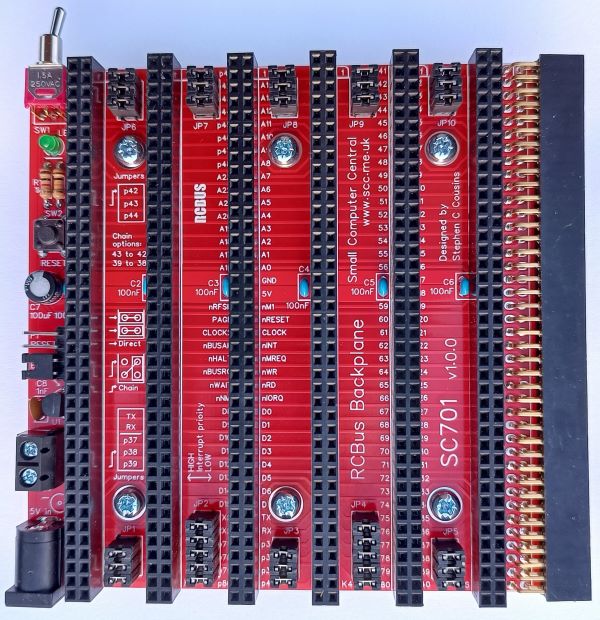
SC701 is an RCBus modular backplane with 6 vertical bus sockets, 1 horizontal bus socket, and a 5-volt power input.
A 12-slot version of this backplane is also available: SC709
- SC701 – Assembly guide
- SC701 – Compatibility
- SC701 – Parts list
- SC701 – Printed circuit board
- SC701 – User guide
- SC700 series information
- SC700 series support
Downloads
- SC701, v1.0, Kit contents sheet (PDF)
- SC701, v1.0, Schematic (PDF)
- SC701, v1.0, PCB design files (OSHWLab)
- SC701, v1.0, Gerber files (ZIP)
- SC701, 3D printed mounting rails at thingiverse.com
Warnings
Assembly: Ensure the bus sockets are pressed firmly against the PCB alone their entire length
Errata
Nothing known
Suppliers
| Kits | Website | From | Currency |
| Small Computers Direct | SCDirect | UK | GBP |
| Stephen C Cousins | Tindie | UK | USD |
| Small Computer Central | Lectronz | UK | Euro/USD |
| PCBs | Website | From | Currency |
| Small Computers Direct | SCDirect | UK | GBP |
| Stephen C Cousins | Tindie | UK | USD |
| Small Computer Central | Lectronz | UK | Euro/USD |
| Assembled and Tested | Website | From | Currency |
| Not available | |||
| Components | |||
| See parts list |
Tindie does not collect VAT for EU countries
Lectronz does collect EU VAT for orders up to 150 EUR
Parts List
| Reference | Qty | Component |
| PCB | 1 | SC701, v1.0, PCB |
| C1 to C6 | 6 | Capacitor, ceramic, 100 nF |
| C7 | 1 | Capacitor, electrolytic, 100 µF |
| C8 | 1 | Capacitor, ceramic, 1 nF |
| JP0 plus P1 | 1 | Header, male, 1 row x 4 pin, angled |
| JP1, 3 and 5 JP6 to JP10 | 8 | Header, male, 2 row x 3 pin, straight |
| JP2 and 4 | 2 | Header, male, 2 row x 5 pin, straight |
| Jumper | 35 | Jumper shunt |
| J1 | 1 | Socket, power, barrel, 2.1mm |
| J2 | 1 | Screw terminal, 2 way, 5.08mm pitch |
| K1 to K6 | 6 | Header, female, 2 row x 40 pin, straight |
| LED1 | 1 | LED, green, 3mm |
| P1 | see JP0 | |
| R1 | 1 | Resistor, 1k, 0.25W |
| R2 | 1 | Resistor, 10k, 0.25W |
| S1 | 1 | Header, female, 2 row x 40 pin, angled |
| SW1 | 1 | Switch, toggle, sub-miniature, SPDT |
| SW2 | 1 | Switch, tactile button, straight |
| U1 | 1 | DS1233-5+ supervisor |
| Spacer | 6 | Spacer, 10mm, M3, nylon |
| Screw (for spacer) | 12 | Machine screw, 6mm, M3 |
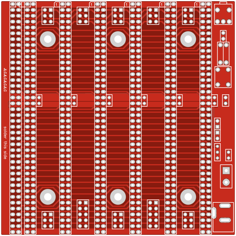
Printed Circuit Board
User Guide
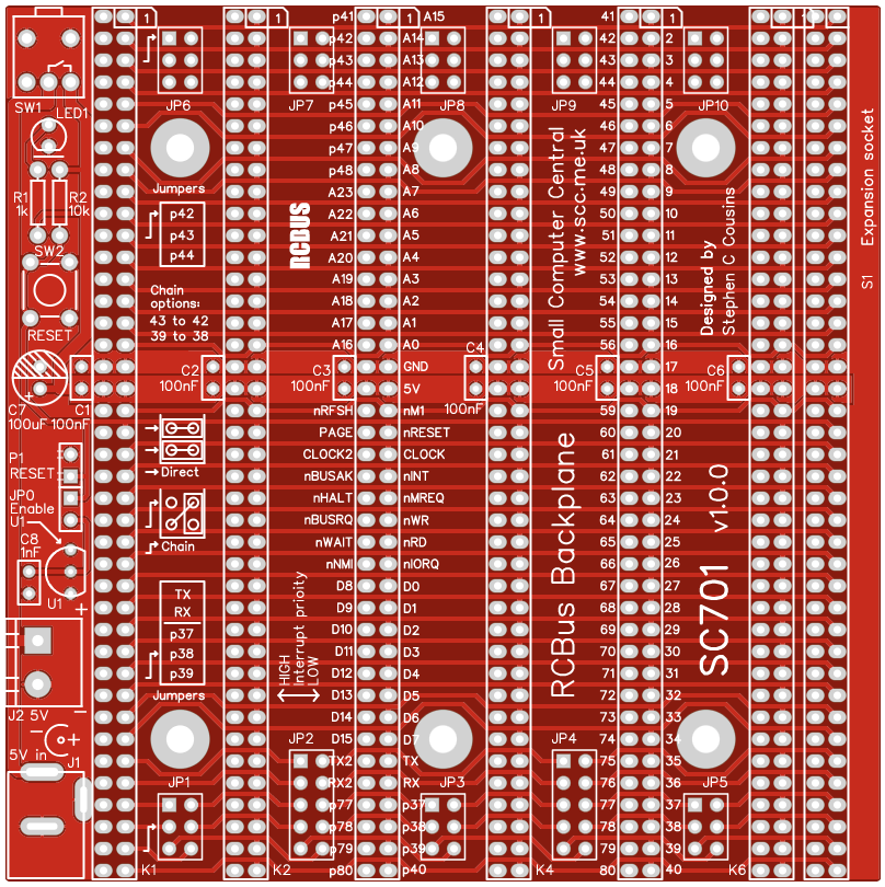
The backplane can supply power to the whole RCBus system by connecting a regulated 5 volt supply to either J1 or J2. J1 is a 2.1mm barrel socket, centre positive, while J2 is a pair of screw terminals.
The regulated 5 volt supply must provide a voltage between 4.75 and 5.25 volts, and must be able to maintain that voltage at the maximum current drawn by the RCBus system, typically 500 mA, but possibly higher.
Power is connected to the modules when the ON/OFF switch, SW1, is in the ON position. The LED lights
Header pins P1 allow an external reset switch to be connected to the backpane.
The voltage supervisor and reset device (U1) provides a reliable power up reset. It works by holding the CPU in reset until the supply voltage reaches approximately 4.75 volts. If the system does not seem to be working, always check the supply voltage is above 4.75 volts on the PCB and that the RESET signal is a logic high voltage, typically above 4 volts. The supervisor should hold the reset low of about 0.5 seconds after the system is turned on and after the reset button is released.
The system should only include one enabled voltage supervisor, so the backplane includes header pins, JP0, to enable the supervor to be connected (jumper shunt fitted) or disabled (jumper shunt not fitted). Normally, it should be connected, but if you have a supervisor on another module you may need to isolate this one.
Input/output port functions
| I/O Address | Read | Write |
| none | n/a | n/a |
Jumper options
| Jumper | Function |
| JP0 | Connect voltage supervisor, U1, to the reset signal |
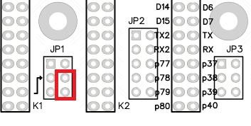
| JP 1, 3, 5 | JPx.1 Connect P37 signal between bus sockets JPx.2 Connect P38 signal between bus sockets* JPx.3 Connect P39 signal between bus sockets* * See daisy chain details below |
| JP 2, 4 | JPx.1 Connect TX signal between bus sockets JPx.2 Connect RX signal between bus sockets JPx.3 Connect P37 signal between bus sockets JPx.4 Connect P38 signal between bus sockets* JPx.5 Connect P39 signal between bus sockets* * See daisy chain details below |
| JP6 to 10 | JPx.1 Connect P42 signal between bus sockets* JPx.2 Connect P43 signal between bus sockets* JPx.3 Connect P44 signal between bus sockets * See daisy chain details below |
JP 1 to JP10 allow some signals to be isolated between bus sockets. This can be helpful if there are several modules that use these signals for different functions.
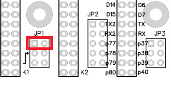
Typically the signals will be connected straight through to each bus socket by fitting jumper shunts horizontally, as illustrated to the left.
Alternatively, a daisy chain can be created from pin 39 to 38. This requires a jumper shunt to be fitted in the position illustrated to the left. A second daisy chain can be created from pin 43 to 42.
A daisy chain is created with two pins on each module. One pin is an output signal while the other is an input signal. The jumper connects the output of one module to the input of the next. The illustration below shows the jumper positions required to create a daisy chain between four modules, in bus sockets K1 to K4.
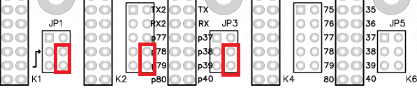
Daisy chains are typically use to create a priority ‘chain’. In the case illustrated above the output is from pin 39 of one module and this is connected to the input pin 38 on the input of module to the right. This creates a priority chain where the modules on the left are a higher priority than modules on the right.
Typical uses for a daisy chain are the Z80 mode 2 interrupt priority, IEI and IEO signals. This is specified as using pins 39 and 38. The second chain, using pins 43 and 42 can be used for a DMA priority chain.
Priority chains require all bus slots in the chain to be occupied by suitable modules. A gap can be left by fitting a pair of jumper shunts horizontally to pass the input and output signals straight through to the bus socket not use the chain signals, rather than being crossed from output to input pins.
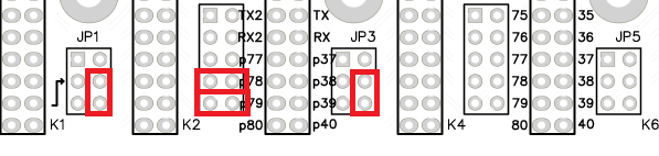
The illustration above configures the backplane for a daisy chain where bus socket K3 does not receive a crossed chain signal and thus should not contain a module which is part of the chain. Socket K3 can be empty or can contain a module which does not have connections to pins 39 or 38.
Assembly Guide
Below is the suggested order of assembly. A general guide to assembling circuit boards can be found here.
- Resistors R1 and R2
These can be fitted either way around - Decoupling capacitors C1 to C6
These can be fitted either way around - Capacitor C8
This can be fitted either way around - Header pins JP0 plus P1
- Switch SW2
- Switch SW1
- Capacitor C7
This must be fitted the correct way around, as described here - Bus socket S1
- Header pins JP1 to JP10
- Bus sockets K1 to K6
Ensure the bus sockets are pressed firmly against the PCB along their entire length - Barrel socket J1
- Screw terminal J2
- LED1
This must be fitted the correct way around, as described here - Voltage supervisor U1
Carefully bend the legs to match the hole spacing on the PCB and ensure the orientation matches the markings on the PCB
Compatibility
This backplane conforms fully to the RCBus specification v1.0 and thus supports: RCBus-2014, RCBus-Z80, RCBus-68xx, RCBus-9995.
The RCBus specification includes RCBus-2014 (both RC2014 standard 40-pin bus and RC2014 enhanced 60-pin bus) and also the full 80-pin RCBus. The 80-pin RCBus provides support for advanced Z80 features, such as the interrupt daisy-chain, as well as support for other processor families.
The following table indicates electrical compatibility with SC701. Check firmware and software details for any required software support.
| Product (80-pin) | ? | Compatibility notes |
| SC126 Z180 motherboard |  | No male header pins for expansion |
| SC701 Backplane 6+1 | | No male header pins for expansion |
| SC702 Backplane 6+1 |  | Adds 6 module sockets RCBus 80-pin |
| SC703 Power from 12v | | Remove jumper shunt JP0 on SC701 |
| SC704 I2C bus master | | Adds I2C bus master and I2C EEPROM |
| SC705 Serial ACIA | | Adds one serial port Typically set to 0x40 |
| SC706 Z80 CPU | | Adds Z80 CPU and main bus clock |
| SC707 Memory 128k | | Adds 128k RAM and 128k flash ROM |
| SC708 Z80 SBC | | Adds CPU, ROM, RAM clock and reset |
| SC709 Backplane 12+1 | | No male header pins for expansion |
| SC710 Backplane 12+1 | | Adds 12 module sockets RCBus 80-pin |
| SC711 Prototyping | | Prototyping module |
| SC712 Power from 5v | | Remove jumper shunt JP0 on SC701 |
| SC713 RCBus tool | n/a | Simple reference tool No electrical function |
| SC714 Memory 512k | | Adds 512k RAM and 512k flash ROM |
| SC715 Compact flash | | Adds Compact Flash storage |
| SC716 Z80 SIO/2 | | Adds two serial ports Typically set to 0x84 |
| SC717 Z80 PIO | | Adds parallel I/O using Z80 PIO |
| SC718 Z80 CTC | | Adds counter/timer using Z80 CTC |
| SC719 Digital I/O | | Adds digital I/O Eight in, eight out |
| SC720 Z80 motherboard | | No male header pins for expansion |
| SC721 Memory 512k | | Adds 512k RAM and 2 x 512k flash ROM |
| SC722 Z180 CPU | | Adds Z180 CPU with two serial ports |
| SC723 Backplane 3 | | No male header pins for expansion |
| SC724 Breakout | | Prototyping breakout module |
| SC725 SIO+CTC | | Adds two serial ports and 4 counter/timers |
| SC726 Clock generator | | Generates CLK and CLK2 bus signals |
| SC727 Real time clock | | Adds real time clock for time and date |
| SC728 Module riser | | Simple module riser for RCBus 80-pin |
| SC791 Z80 system | | No male header pins for expansion |
| SC792 Z180 system | | No male header pins for expansion |
| Product (40 pin) | ? | Compatibility notes |
| SC114 Z80 motherboard | | No male header pins for expansion |
| SC130 Z180 motherboard | | No male header pins for expansion |
| SC133 Backplane 11+1 | | No male header pins for expansion |
| SC134 LED output port | | Adds eight LED outputs |
| SC135 Digital output port | | Adds eight digital outputs |
| SC136 Digital input port | | Adds eight digital inputs |
| SC137 I2C bus master | | Adds I2C bus master |
| SC139 Serial ACIA | | Adds one serial port Typically set to 0x40 |
| SC141 Backplane 12+1 | | Adds 12 module sockets RCBus 40-pin |
| SC142 Power from 12v | | Remove jumper shunt JP0 on SC701 |
| SC143 Flash ROM | | Adds 128k flash ROM |
| SC145 Compact flash | | Adds Compact Flash storage |
| SC147 Backplane 6+1 | | Adds 6 module sockets RCBus 40-pin |
| SC148 Power from 5v | | Remove jumper shunt JP0 on SC701 |
| SC149 Z80 CPU | | Adds Z80 CPU and main bus clock |
| SC150 Paged RAM 128k | | Adds 128k of paged RAM |
| SC151 Paged ROM 128k | | Adds 128k of paged ROM |
| Other suppliers | ? | Compatibility notes |
| RC2014 Mini system | | No male header pins for expansion |
| RC2014 Pro system | | No male header pins for expansion |
| RC2014 Zed system | | No male header pins for expansion |
| RC2014 Micro module | | Adds CPU, ROM, RAM serial, clock and reset |
| RC2014 Backplane 5 | | If header pins fitted it adds 4 x 40-pin sockets |
| RC2014 Backplane 8 | | No male header pins for expansion |
| RC2014 Backplane Pro | | No male header pins for expansion |
| RC2014 Z80 CPU | | Adds Z80 CPU |
| RC2014 SIO/2 dual serial | | Adds two serial ports at 0x80 to 0x87 |
| RC2014 Compact flash | | Adds Compact Flash at 0x10 to 0x17 |
| RC2014 Dual clock | | Generates CLK and CLK2 bus signals |
| RC2014 Pageable ROM | | Adds 64k paged ROM |
| RC2014 64k RAM | | Adds 64k paged RAM |
| RC2014 Memory 512k | | Adds 512k RAM and 512k flash ROM |
| RC2014 Digital I/O | | Adds eight LED outputs and eight push buttons |
| RC2014 Real time clock | | Adds real time clock for time and date |
| RC2014 RP2040 VGA terminal | | Connect VGA monitor and USB keyboard |
| RC2014 Pi Pico terminal | | Connect VGA monitor and USB keyboard |
| RC2014 YM2149 sound card | | Adds authentic retro sound |
| Weird electronics Flock v2 | | Adds floppy disk and real time clock |
Notes
- This product is designed for hobby use and is not suitable for industrial, commercial, or safety-critical applications.
- The product contains small parts and is not suitable for young children.
