SC718 is a Z80 CTC (Counter Timer Channels) module designed for the RCBus. It is provides a 4 channel timer, counter, frequency generator and Z80 mode 2 interrupt generator.

- SC718 – Assembly guide
- SC718 – Compatibility
- SC718 – Parts list
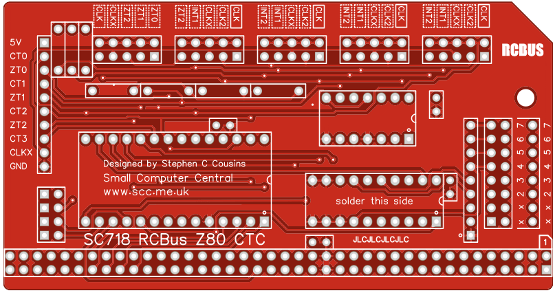
- SC718 – Printed circuit board
- SC718 – User guide
- SC700 series information
- SC700 series support
Downloads
- SC718, v1.0, Kit contents sheet (PDF)
- SC718, v1.0, Schematic (PDF)
- SC718, v1.0, PCB design files (OSHWLab)
- SC718, v1.0, Gerber files (ZIP)
Errata
- PCB SC718 v1.0.0 has the wrong part number label for U2. Fixed in PCB v1.0.1
Suppliers
| Kits | Website | From | Currency |
| Small Computers Direct | SCDirect | UK | GBP |
| Stephen C Cousins | Tindie | UK | USD |
| Small Computer Central | Lectronz | UK | Euro/USD |
| PCBs | Website | From | Currency |
| Small Computers Direct | SCDirect | UK | GBP |
| Stephen C Cousins | Tindie | UK | USD |
| Small Computer Central | Lectronz | UK | Euro/USD |
| Assembled and Tested | Website | From | Currency |
| Not available | |||
| Components | |||
| See parts list |
Tindie does not collect VAT for EU countries
Lectronz does collect EU VAT for orders up to 150 EUR
Parts List
| Reference | Qty | Component |
| PCB | 1 | SC718, v1.0, PCB |
| C1 to C4 | 4 | Capacitor, ceramic, 100 nF |
| JP1 | 1 | Header, male, 2 row x 8 pin, angled |
| JP2+3+4+5+6 | 1 | Header, male, 2 row x 29 pin, straight *2 (some pins need to be removed) |
| JP7+8+9+10 | 1 | Header, male, 2 row x 4 pin, angled, or Header, male, 2 row x 4 pin, straight *1 |
| Jumpers | 15 | Jumper shunts |
| P1 | 1 | Header, male, 2 row x 40 pin, angled |
| P2 | 1 | Header, male, 1 row x 10 pin, angled |
| R1 to R4 | 4 | Resistor, 1M, 0.25W |
| R5 to R7 | 3 | Resistor, 10k, 0.25W |
| RN1 | 1 | Resistor network, 8x100k, SIL, 9-pin |
| Screw (for spacer) | 1 | Machine screw, 6mm, M3 |
| Spacer | 1 | Spacer, 10mm, M3, nylon |
| U1 | 1 | 74HCT688 |
| U2 | 1 | Z80 CTC Z84C3008, or Z80 CTC Z84C3010 |
| X1 | 1 | Oscillator (optional) Not included in the kit |
| IC socket 20-pin U1 | 1 | Socket, DIP, 20-pin |
| IC socket 28-pin U2 | 2 | Socket, DIP, 28-pin |
- If you don’t need to connect flying leads (eg. Dupont wire) to IEI and IEO you could use straight pins rather than angled pins. You only need flying leads on these pins if you want to create an interrupt daisy chain and the backplane does not support this feature. Backplanes designed to meet the full requirements of the RCBus v1.0 provide for this with jumpers.
- You could fit angled header pins if you want easy access to these jumper settings but they obscure the labels and protrude beyond the edge of the PCB.
Printed Circuit Board

User Guide
SC718 is a Z80 CTC (Counter Timer Channels) module designed for the RCBus. It is provides a 4 channel timer, counter, frequency generator and Z80 mode 2 interrupt generator.
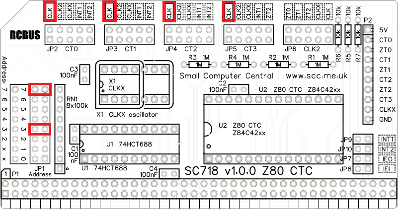
The device address is set with jumpers. All of the I/O pins are available on header pins on the back edge of the PCB on on the RCBus.
The input source for each channel is selected with a jumper. Input sources include the RCBus CLK and CLK2 signals, the onboard oscillator, and the RCBus INT1 and INT2 signals.
The CTC can generate clock signals at programmable frequencies, such as baud rate clocks. A jumper allows the CTC to generate a clock on the RCBus CLK2 pins.
The CTC can generate Z80 mode 2 interrupts for non-Z80 family devices. The RCBus-Z80 provides two interrupt pins for non-Z80 devices. Jumpers allow these interrupts to be connected to the CTC which can be programmed to detect appropriate edges and generate interrupts.
A periodic timer interrupt can be generated by any of the channels. A jumper allows the output of channel 2 to be connected to the input of channel 3, thus providing a 16-bit timer. Alternatively, channel 3 can count timer ticks from timer 2 providing a means of detecting missed interrupts.
The Z80 interrupt daisy chain can be implemented on a backplane conforming to the RCBus-Z80 specification or it can be implemented via Dupont style wires connected the the IEI and IEO header pins.
Details about programming a Z80 CTC can be found in the Z80 CTC datasheet (PDF).
Input/output port functions
| I/O Address | Read | Write |
| Configurable *1 base address | Read Z80 CTC | Write Z80 CTC |
| base + 0 | CTC 0 | CTC 0 |
| base + 1 | CTC 1 | CTC 1 |
| base + 2 | CTC 2 | CTC 2 |
| base + 3 | CTC 3 | CTC 3 |
- The RCBus I/O base address should be set to match the software you are using. Typically, this is 0x88 (binary 1000 1000).
Jumper options
| Jumper | Function |
| JP 1 | Set module’s RCBus I/O base address The suggested address is 0x88 (binary 1000 1000) |
| JP 2 | CTC channel 0 input source (CT0) JP2.1 – RCBus clock signal (CLK) JP2.2 – RCBus clock 2 signal (CLK2) JP2.3 – Onboard oscillator output (X1) JP2.4 – RCBus interrupt 1 signal (/INT1) JP2.5 – RCBus interrupt 2 signal (/INT2) The default is RCBus clock signal (CLK) |
| JP 3 | CTC channel 1 input source (CT1) JP3.1 – RCBus clock signal (CLK) JP3.2 – RCBus clock 2 signal (CLK2) JP3.3 – Onboard oscillator output (X1) JP3.4 – RCBus interrupt 1 signal (/INT1) JP3.5 – RCBus interrupt 2 signal (/INT2) The default is RCBus clock signal (CLK) |
| JP 4 | CTC channel 2 input source (CT2) JP4.1 – RCBus clock signal (CLK) JP4.2 – RCBus clock 2 signal (CLK2) JP4.3 – Onboard oscillator output (X1) JP4.4 – RCBus interrupt 1 signal (/INT1) JP4.5 – RCBus interrupt 2 signal (/INT2) The default is RCBus clock signal (CLK) |
| JP 5 | CTC channel 3 input source (CT3) JP5.1 – RCBus clock signal (CLK) JP5.2 – RRCBus clock 2 signal (CLK2) JP5.3 – Onboard oscillator output (X1) JP5.4 – RCBus interrupt 1 signal (/INT1) JP5.5 – CTC 2 output (ZT2) The default is RCBus clock signal (CLK) |
| JP 6 | Signal output to RCBus clock 2 signal (CLK2) JP6.1 – CTC channel 0 output (ZT0) JP6.2 – CTC channel 1 output (ZT1) JP6.3 – CTC channel 2 output (ZT2) JP6.4 – Onboard oscillator output (X1) JP6.5 – RCBus clock signal (CLK) The default is jumper shunt not fitted |
| JP 7 | Connects RCBus IEO signal to module The default is jumper shunt not fitted |
| JP 8 | Connects RCBuss IEI signal to module The default is jumper shunt not fitted |
| JP 9 | Connects RCBus INT signal to module The default is jumper shunt not fitted |
| JP 10 | Connects RCBus INT2 signal to module The default is jumper shunt not fitted |
Assembly Guide
Below is the suggested order of assembly. A general guide to assembling circuit boards can be found here.
- Resistors R1 to R7
These can be fitted either way around - Decoupling capacitors C1 to C4
These can be fitted either way around - Sockets for U1 and U2
Fit such that the notch in the socket matches the curve in the outline on the PCB silkscreen - Header pins P2
- Bus header P1
Make sure the pins are parallel to the PCB so that the board is vertical when it is fitted into a backplane socket - Resistor network RP1
This must be fitted the correct way around whereby the dot on the component matches the dot on the PCB silkscreen - Header pins JP1
- Header pins JP2+JP3+JP4+JP5+JP6
This can be fitted as one strip if pin pairs 6, 12, 18 and 24 are pulled out of the plastic with a pair of pliers
See parts list for options - Header pins JP7+JP8+JP9+JP10
See parts list for options - Insert the integrated circuits into their sockets
Make sure the notch in the component is at the end indicated by the notch in the socket and the curve on the PCB silkscreen - Fit the nylon spacer in the mounting hole
Fit jumper shunts in the positions shown below. All other jumpers are optional and should only be fitted if the feature is required.
Compatibility
This module conforms to the RCBus specification v1.0 for RCBus-2014 and RCBus-Z80.
The RCBus specification includes RCBus-2014 (both RC2014 standard 40-pin bus and RC2014 enhanced 60-pin bus) and also the full 80-pin RCBus. The 80-pin RCBus provides support for advanced Z80 features, such as the interrupt daisy-chain, as well as support for other processor families.
The table below indicates electrical compatibility with each backplane type (40, 60 and 80 pin)

| Backplane | ? | Compatibility notes |
| RCBus 80-pin |  | Fully supported |
| RCBus 60-pin (RC2014 enhanced) | | Limitations: Optional mode 2 interrupt chain requires wires between modules |
| RCBus 40-pin (RC2014 standard) | | Limitations: Optional mode 2 interrupt chain requires wires between modules Some optional signals are not available (CLK2, /INT2) |
Notes
- This product is designed for hobby use and is not suitable for industrial, commercial, or safety-critical applications.
- The product contains small parts and is not suitable for young children.
