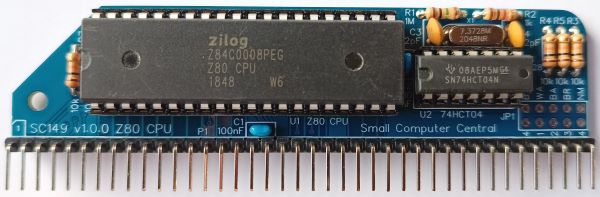
SC149 is a Z80 CPU and clock module designed for the RC2014 bus.
- SC149 – Assembly Guide
- SC149 – Parts List
- SC149 – Printed Circuit Board
- SC149 – Suppliers
- SC149 – Support
- SC149 – User Guide
Downloads
- SC149 – Kit contents sheet (PDF)
- SC149 – Schematic v1.0 (PDF)
- SC149 – PCB design files v1.0 (OSHWLab)
- SC149 – Gerber files v1.0 (ZIP)
Suppliers
| Kits | Website | From | Currency |
| Small Computers Direct | SCDirect | UK | GBP |
| Stephen C Cousins | Tindie | UK | USD |
| PCBs | Website | From | Currency |
| Small Computers Direct | SCDirect | UK | GBP |
| Stephen C Cousins | Tindie | UK | USD |
| Assembled and Tested | Website | From | Currency |
| Not available | |||
| Components | |||
| See parts list |
Parts List
| Reference | Qty | Component | |
| PCB | 1 | SC149, v1.0, PCB | |
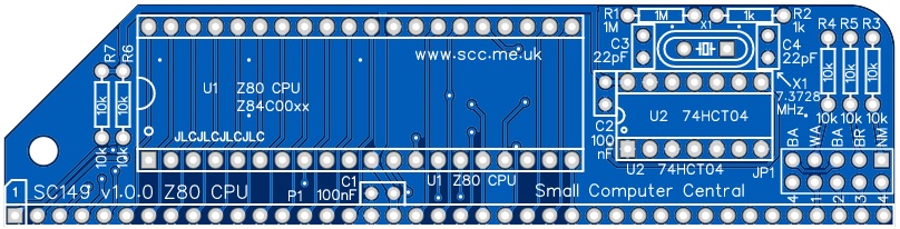
| C1 and C2 | 2 | Capacitor, ceramic, 100 nF | |
| C3 and C4 | 2 | Capacitor, ceramic, 22 pF | |
| JP1 | 1 | Header, male, 2 row x 5 pin, straight | |
| Jumper | 4 | Jumper shunt | |
| P1 | 1 | Header, male, 1 row x 40 pin, angled | |
| R1 | 1 | Resistor, 1M, 0.25W | |
| R2 | 1 | Resistor, 1k, 0.25W | |
| R3 to R7 | 5 | Resistor, 10k, 0.25W | |
| U1 | 1 | Z80 CPU Z84C0008PEG, or Z80 CPU Z84C0010PEG | |
| U2 | 1 | 74HCT04 | |
| U1 socket | 1 | 40-pin DIP socket | |
| U2 socket | 1 | 14-pin DIP socket | |
| X1 | 1 | Crystal, 7.3728MHz |
Printed Circuit Board

User Guide
SC149 provides a Z80 Central Processing Unit (CPU) and a clock oscillator, typically 7.3728 MHz.
If you want to use this module without using the onboard clock oscillator, simply remove the 74HCT04 (U2).
Being a 40-pin standard bus module there are a few Z80 signals that are not available on the bus. These include /NMI, /BUSRQ, /BUSAK, and /WAIT. Most systems will not require these signals but if they are needed they are available on JP1. Either these signals can be connected to specific USER pins on the bus or can be connected with flying leads, such as a Dupont cables.
Input/output port functions
| I/O Address | Read | Write |
| none | n/a | n/a |
Jumper options
| Jumper | Function | Label |
| JP1 | User pin bus signals JP1.1 connects USER4 to /NMI (NM) JP1.2 connects USER3 to /BUSRQ JP1.3 connects USER2 to /BUSAK JP1.4 connects USER1 to /WAIT JP1.5 connects USER4 to /BUSAK | 4 – NM 3 – BR 2 – BA 1 – WA 4 – BA |
It is recommended that jumper shunts not be fitted unless you have a specific need and have checked no other signals are connected to the same USER bus pins.
Assembly Guide
Below is the suggested order of assembly. A general guide to assembling circuit boards can be found here.
- Resistors R1 to R7
These can be fitted either way around - Sockets for U1 and U2
Fit such that the notch in the socket matches the curve in the outline on the PCB silkscreen - Bus header P1
Make sure the pins are parallel to the PCB so that the board is vertical when it is fitted into a backplane socket - Capacitors C1 to C4
These can be fitted either way around - Crystal X1
This can be fitted either way around - Header JP1
Most systems will not need these so best left unconnected until needed - Insert the integrated circuits into their sockets
Make sure the notch in the component is at the end indicated by the notch in the socket and the curve on the PCB silkscreen
Notes
- This design is made in accordance with the “designed for RC2014” labelling scheme.
- RC2014 is a trademark of RFC2795 Ltd.
- This product is designed for hobby use and is not suitable for industrial, commercial, or safety-critical applications.
- The product contains small parts and is not suitable for young children.
