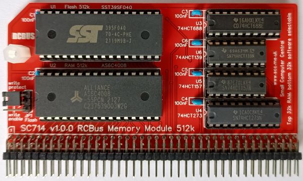
SC714 is a memory module with 512k bytes of FLASH ROM and 512k pages of RAM designed for the RCBus. This module provides suitable memory for running RomWBW and CP/M.
- SC714 – Assembly guide
- SC714 – Compatibility
- SC714 – Firmware, RomWBW RCZ80_std
- SC714 – Firmware, SCM S7
- SC714 – Parts list
- SC714 – Printed circuit board
- SC714 – User guide
- SC700 series information
- SC700 series support
Downloads
- SC714, v1.0, Kit contents sheet (PDF)
- SC714, v1.0, Schematic (PDF)
- SC714, v1.0, PCB design files (OSHWLab)
- SC714, v1.0, Gerber files (ZIP)
Errata
Nothing known
Suppliers
| Kits | Website | From | Currency |
| Small Computers Direct | SCDirect | UK | GBP |
| Stephen C Cousins | Tindie | UK | USD |
| Small Computer Central | Lectronz | UK | Euro/USD |
| PCBs | Website | From | Currency |
| Small Computers Direct | SCDirect | UK | GBP |
| Stephen C Cousins | Tindie | UK | USD |
| Small Computer Central | Lectronz | UK | Euro/USD |
| Assembled and Tested | Website | From | Currency |
| Not available | |||
| Components | |||
| See parts list |
Tindie does not collect VAT for EU countries
Lectronz does collect EU VAT for orders up to 150 EUR
Parts List
| Reference | Qty | Component |
| PCB | 1 | SC714, v1.0, PCB |
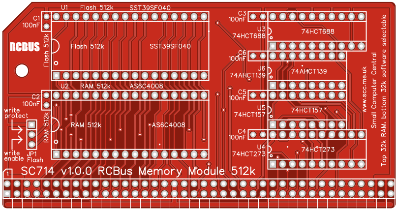
| C1 to C6 | 6 | Capacitor, ceramic, 100 nF |
| JP1 | 1 | Header, male, 1 row x 3 pin, angled |
| Jumper | 1 | Jumper shunt |
| P1 | 1 | Header, male, 2 row x 40 pin, angled |
| Screw (for spacer) | 1 | Machine screw, 6mm, M3 |
| Spacer | 1 | Spacer, 10mm, M3, nylon |
| U1 | 1 | FLASH 512k bytes SST39SF040 |
| U2 | 1 | RAM 512k bytes AS6C4008 |
| U3 | 1 | 74HCT688 |
| U4 | 1 | 74HCT273 |
| U5 | 1 | 74HCT157 |
| U6 | 1 | 74AHCT139 |
| IC socket 32-pin U1 and U2 | 2 | Socket, DIP, 32-pin |
| IC socket 20-pin U3 and U4 | 2 | Socket, DIP, 20-pin |
| IC socket 16-pin U5 and U6 | 2 | Socket, DIP, 16-pin |
Printed Circuit Board

User Guide
SC714 provides 512k bytes of banked FLASH ROM and 512k bytes of banked RAM, together with paging control of the lower 32k. This configuration is suitable for running RomWBW and CP/M.
The top 32k bytes of the 512k byte RAM are always mapped to the top 32k bytes of the Z80’s memory space (0x8000 to 0xFFFF).
At reset the bottom 32k bytes of the 512k byte FLASH ROM are mapped to the bottom 32k bytes of the Z80’s memory space (0x0000 to 0x7FFF).
Any of the sixteen 32k byte FLASH ROM banks (0 to 15) or any of the sixteen 32k byte RAM banks (16 to 31) can be mapped to the bottom 32k bytes of the Z80’s memory space (0x0000 to 0x7FFF) with a single write to I/O address 0x78 (or 0x79). The value written to this I/O address is two times the bank number. Bits 0, 6 and 7 are ignored. This scheme has been used for compatibility with existing software.
Input/output port functions
| I/O Address | Read | Write |
| 0x78 (0x78 to 0x79) | n/a | Memory bank select Bits 1 to 5 = Bank number (x2) Bit 5 = RAM (hi), FLASH (lo) |
Jumper options
| Jumper | Function |
| JP1 | FLASH write enable / protect Read only = Write protected Write = Read and write enabled |
It is recommended that a jumper shunt be fitted in the “Read only” position of JP1 during normal use. It only needs to be in the “Write” position when the contents of the FLASH is to be updated. While the FLASH device requires a very specific sequence of events to protect it against accidental modification, it is best to play safe and use the jumper to ensure it can not be written to.
Assembly Guide
Below is the suggested order of assembly. A general guide to assembling circuit boards can be found here.
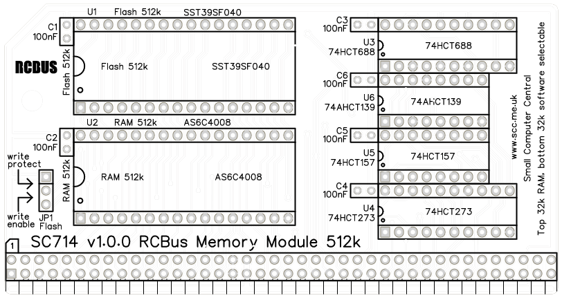
- Decoupling capacitors C1 to C6
These can be fitted either way around - Sockets for U1 to U6
Fit such that the notch in the socket matches the curve in the outline on the PCB silkscreen - Bus header P1
Make sure the pins are parallel to the PCB so that the board is vertical when it is fitted into a backplane socket - Header pins JP1
- Insert the integrated circuits into their sockets
Make sure the notch in the component is at the end indicated by the notch in the socket and the curve on the PCB silkscreen - Fit the nylon spacer in the mounting hole
Fit a jumper shunt in the position shown below.

Compatibility
This module conforms to the RCBus specification v1.0 for RCBus-2014 and RCBus-Z80.
The RCBus specification includes RCBus-2014 (both RC2014 standard 40-pin bus and RC2014 enhanced 60-pin bus) and also the full 80-pin RCBus. The 80-pin RCBus provides support for advanced Z80 features, such as the interrupt daisy-chain, as well as support for other processor families.
Compatible with Z80 CPU module SC706, but not with Z80 CPU module SC730.
The table below indicates electrical compatibility with each backplane type (40, 60 and 80 pin)

| Backplane | ? | Compatibility notes |
| RCBus 80-pin |  | Fully supported |
| RCBus 60-pin (RC2014 enhanced) | | Fully supported |
| RCBus 40-pin (RC2014 standard) | | Fully supported |
Notes
- This product is designed for hobby use and is not suitable for industrial, commercial, or safety-critical applications.
- The product contains small parts and is not suitable for young children.
- RomWBW is copyright Wayne Warthen and has been provided free of charge with his permission.
