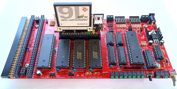
SC720 is a Z80 Single Board Computer (SBC) in a motherboard format. It can run RomWBW, CP/M and the Small Computer Monitor (SCM).

- SC720 – Assembly guide
- SC720 – Compatibility
- SC720 – Firmware, RomWBW RCZ80_std
- SC720 – Firmware, SCM S7
- SC720 – Parts list
- SC720 – Printed circuit board
- SC720 – User guide
- SC700 series information
- SC700 series support
Downloads
- SC720, v1.0, Kit contents sheet (PDF)
- SC720, v1.0, Schematic (PDF)
- SC720, v1.0, PCB design files (OSHWLab)
- SC720, v1.0, Gerber files (ZIP)
Errata
See notes about the Compact Flash adapter.
Suppliers
| Kits | Website | From | Currency |
| Small Computers Direct | SCDirect | UK | GBP |
| Stephen C Cousins | Tindie | UK | USD |
| Small Computer Central | Lectronz | UK | Euro/USD |
| PCBs | Website | From | Currency |
| Small Computers Direct | SCDirect | UK | GBP |
| Stephen C Cousins | Tindie | UK | USD |
| Small Computer Central | Lectronz | UK | Euro/USD |
| Assembled and Tested | Website | From | Currency |
| Not available | |||
| Components | |||
| See parts list |
Tindie does not collect VAT for EU countries
Lectronz does collect EU VAT for orders up to 150 EUR
Parts List
| Reference | Qty | Component |
| PCB | 1 | SC720, v1.0, PCB |
| C1 to C17 | 17 | Capacitor, ceramic, 100 nF |
| C18 and C19 | 2 | Capacitor, ceramic, 22 pF |
| C20 to C22 | 3 | Capacitor, electrolytic, 100 µF |
| C23 | 1 | Capacitor, ceramic, 1 nF |
| D1 | 1 | Diode, 1N4001 |
| JP1 and JP2 | 2 | Header, male, 1 row x 3 pin, straight |
| JP3 + JP4 JP5 + JP6 JP7 + JP8 | 3 | Header, male, 2 row x 3 pin, straight |
| JP9 + JP10 | 1 | Header, male, 2 row x 2 pin, straight |
| JP11 and JP12 | 2 | Header, male, 2 row x 3 pin, straight |
| JP13 | 1 | Header, male, 1 row x 2 pin, straight |
| Jumper | 17 | Jumper shunts |
| LED1 to LED10 | 10 | LED, green, 3mm, angled |
| LED11 | 1 | LED, red, 3mm, angled |
| P1 and P2 | 2 | Header, male, 1 row x 6 pin, angled |
| P3 | 1 | Box header, 2 x 20 pin, straight *, or Header, male, 2 x 20 pin, straight * included in the kit |
| P4 and P5 | 2 | Header, male, 1 row x 2 pin, straight |
| R1 to R4 | 4 | Resistor, 1k, 0.25W |
| R5 to R12 | 8 | Resistor, 2k2, 0.25W |
| R13 to R18 | 6 | Resistor, 4k7, 0.25W |
| R19 to R23 | 5 | Resistor, 10k, 0.25W |
| R24 to R30 | 7 | Resistor, 100k, 0.25W |
| R31 | 1 | Resistor, 1M, 0.25W |
| RN1 | 1 | Resistor network, 8x1k, SIL, 9-pin |
| S1 and S2 | 2 | Header, female, 1 row x 6 pin, angled |
| S3 | 1 | Socket, power, barrel, 2.1mm |
| S4 | 1 | Header, female, 2 row x 40 pin, angled |
| S5 and S6 | 2 | Header, female, 2 row x 40 pin, straight |
| ST1 and ST2 | 2 | Screw terminal, 2 way, 5.08mm pitch |
| SW1 | 1 | Switch, toggle, sub-miniature, SPDT |
| SW2 | 1 | Switch, toggle, sub-miniature, SPDT (optional) |
| SW3 | 1 | Switch, tactile button, angled |
| Screw (for spacer) | 8 | Machine screw, 6mm, M3 |
| Spacer | 4 | Spacer, 10mm, M3, nylon |
| Nut (for U17) | 1 | Nut, M3.5 |
| Bold (for U17) | 1 | Bolt, M3.5, 10mm, pan head |
| Heatsink (for U17) | Heatsink TO-220, 19x20x9mm | |
| U1 | 1 | Z80 CPU, Z84C0008PEG, or Z80 CPU, Z84C0010PEG |
| U2 | 1 | RAM 512k bytes AS6C4008 |
| U3 and U4 | 2 | FLASH 512k bytes SST39SF040 |
| U5 | 1 | 74HCT688 |
| U6 and U10 | 2 | 74HCT273 |
| U7 | 1 | 74AHCT139 |
| U8 | 1 | 74HCT157 |
| U9 | 1 | Z80 SIO/2, Z84C4208PEG, or Z80 SIO/2, Z84C4210PEG |
| U11 | 1 | 74HCT125 |
| U12 | 1 | 74HCT74 |
| U13 | 1 | 74HCT32 |
| U14 and U15 | 2 | 74HCT138 |
| U16 | 1 | 74HCT02 |
| U17 | 1 | 7805 regulator, 5V, 1A |
| U18 | 1 | DS1233-5+ supervisor |
| X1 | 1 | 7.3728 MHz crystal |
| IC socket 40-pin U1 and U9 | 2 | Socket, DIP, 40 pin |
| IC socket 32-pin U2 to U4 | 3 | Socket, DIP, 32-pin |
| IC socket 20-pin U5, U6 and U10 | 3 | Socket, DIP, 20-pin |
| IC socket 16-pin U7, U8, U14, U15 | 4 | Socket, DIP, 16-pin |
| IC socket 14-pin U11, U12, U13, U16 | 4 | Socket, DIP, 14-pin |
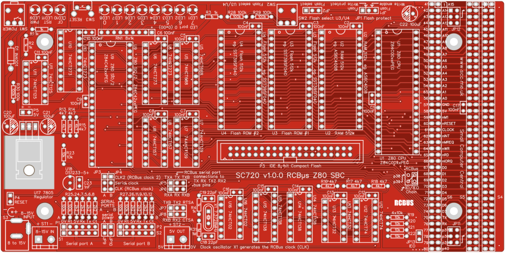
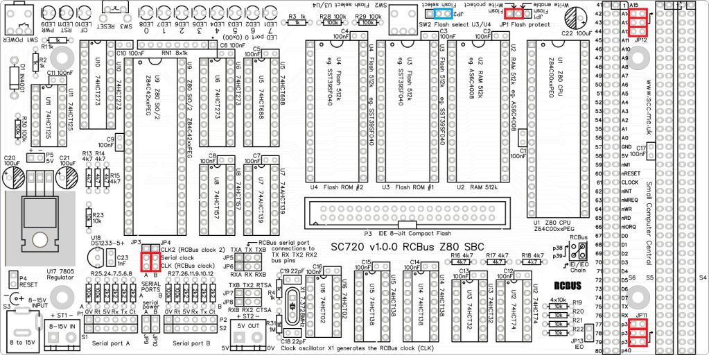
Printed Circuit Board

User Guide
SC720 is a Single Board Computer (SBC) meaning it can work without any other backplanes or modules. It is based on a Z80 CPU running at 7.3728 MHz, with 512k bytes of RAM, two 512k byte of FLASH ROMs, a Z80 SIO/2 provides two serial ports, a Compact Flash card interface, a clean reset, a voltage supervisor, and an output port with eight LEDs. It is powered from an 8 to 15 volt supply at up to 1 amp.
The kit includes RomWBW pre-programmed into a FLASH ROM. This includes CP/M and a range of other software.
The kit also includes the Small Computer Monitor pre-programmed into a FLASH ROM. This includes a capable debug/monitor, BASIC, and a CP/M loader.
Switch SW2 or jumper JP2 allow selection of either flash ROM (U3 or U4), thus allowing selection of either RomWBW or the Small Computer Monitor (SCM).
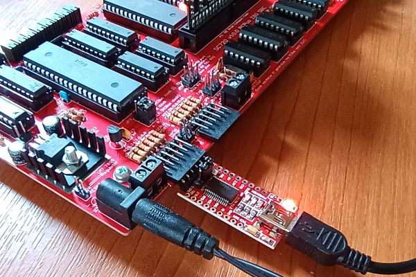
The motherboard is connected to a terminal or computer running terminal emulation software, such as Tera Term. Connection to a computer’s USB port requires a USB to serial adapter, as shown below. This can be connected directly, as shown, or with a 6-way adapter cable.
The serial port settings should normally be 115200 baud, 8 data bits, 1 stop bit, no parity. Basic operations work without flow control but RTS/CTS hardware handshaking should be enabled for reliable file transfers.
A Compact Flash card is optional but highly desirable. The Compact Flash adapter and card are shown below.

Power is supplied by either the barrel socket S3 (2.1mm, centre positive) or the screw terminal block ST1. This should be between 8 and 15 volts D.C. at up to 1 amp. When power is applied and the on/off switch is in the On position then power LED should light.
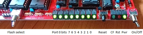
At power up or when the reset button is pressed the red reset LED should light for about half a second, or longer if the reset button is being pressed. The compact flash LED should light when the CF card is being accessed.
The set of 8 LEDs on port 0 should light up in sequence when the system is reset. See firmware for details of the sequence and meaning.
The port 0 LEDs can be controlled from BASIC with the OUT statement or from SCM with the O statement. For example, to turn on bit 0 and bit 1 LEDs from BASIC, type “OUT 0,3” and from SCM “O 0 3”. In assembler the instructions “LD A,3” followed by “OUT (0),A” also lights these LEDs.
The firmware and software documentation can be found using the links at the top of this page.
Input/output port functions
| I/O Address | Read | Write |
| 0x00 (0x00 to 0x03) | n/a | LED port (LED 1 to 8) Low = OFF, high = ON |
| 0x10 (0x10 to 0x17) | Compact Flash Read | Compact Flash Write |
| 0x78 (0x78 to 0x79) | n/a | Memory bank select bits 1 to 5 |
| 0x80 (0x80 to 0x83) | SIO/2 Read | SIO/2 Write |
Z80 SIO/2 register addresses
| I/O Address | Z80 PIO/2 register |
| 0x80 | Port A control |
| 0x81 | Port A data |
| 0x82 | Port B control |
| 0x83 | Port B data |
Jumper options
| Jumper | Function |
| JP 1 | FLASH write enable / protect Write protect = Read only Write enable = Read and write enabled |
| JP 2 | FLASH ROM select Either U3 or U4 Do not fit jumper shunt if switch SW2 is fitted |
| JP 3 | Selects the serial clock source for port A JP 3.1-2 Clock source is bus CLK2 signal JP 3.2-3 Clock source is oscillator X1 The default is X1 |
| JP 4 | Selects the serial clock source for port B JP 4.1-2 Clock source is bus CLK2 signal JP 4.2-3 Clock source is oscillator X1 The default is X1 |
| JP 5 | Connects the bus TX signal to TXA or TXB JP 5.1-2 Connect port A TX signal to bus TX signal JP 5.2-3 Connect port B TX signal to bus TX signal The default is jumper shunt not fitted |
| JP 6 | Connects the bus RX signal to RXA or RXB JP 6.1-2 Connect port A RX signal to bus RX signal JP 6.2-3 Connect port B RX signal to bus RX signal The default is jumper shunt not fitted |
| JP 7 | Connects the bus TX2 signal to TXB or /RTSA JP 7.1-2 Connect port B TX signal to bus TX2 signal JP 7.2-3 Connect port A /RTS signal to bus TX2 signal The default is jumper shunt not fitted |
| JP 8 | Connects the bus RX2 signal to RXB or /CTSA JP 8.1-2 Connect port B RX signal to bus RX2 signal JP 8.2-3 Connect port A /CTS signal to bus RX2 signal The default is jumper shunt not fitted |
| JP 9 | Connects 5 volt power to serial port A connectors The default is jumper shunt not fitted |
| JP 10 | Connects 5 volt power to serial port B connectors The default is jumper shunt not fitted |
| JP 11 | JP 11.1 Connect P37 signal between bus sockets JP 11.2 Connect P38 signal between bus sockets* JP 113. Connect P39 signal between bus sockets* * See daisy chain details below |
| JP 12 | JP12.1 Connect P42 signal between bus sockets* JP12.2 Connect P43 signal between bus sockets* JP12.3 Connect P44 signal between bus sockets * See daisy chain details below |
| JP 13 | Connects bus IEO signal to SIO/2 IEO signal The default is jumper shunt not fitted |
JP 11 and JP 12 allow some signals to be isolated between bus sockets. Also, jumpers allow daisy chains to be created. See backplanes, such as SC701, for details jumper positions).
Assembly Guide
Below is the suggested order of assembly. A general guide to assembling circuit boards can be found here.

See notes about the Compact Flash adapter.
- Resistors R1 to R31
These can be fitted either way around - Diode D1
- This must be fitted the correct way around, with the band on the diode matching the marking on the PCB
- Sockets S1 and S2
Ensure these are fitted flat against the circuit board - Header pins P1 and P2
Ensure the pins are parallel to sockets S1 and S2 - Decoupling capacitors C1 to C17
These can be fitted either way around - Resistor network RN1
This must be fitted the correct way around whereby the dot on the component matches the dot on the PCB silkscreen - Sockets for U1 to U16
Fit such that the notch in the socket matches the curve in the outline on the PCB silkscreen - Capacitors C18 and C19, and also C23
These can be fitted either way around - Switch SW1
- Optional switch SW2
- Capacitors C20 to C22
This must be fitted the correct way around, as described here - Reset light emitting diode LED 11 (red)
The angled LEDs in the kit only fit one way around, but standard LEDs need to have the short lead in the hole marked with a flat line, as described here - LEDs 1 to 10 (green)
- The angled LEDs in the kit only fit one way around, but standard LEDs need to have the short lead in the hole marked with a flat line, as described here
- Push button switch SW3
- Header pins JP3+4, JP5+6, JP7+8, JP9+10, JP11, JP12 (2 row straight pins)
- Header pins JP1, JP2, JP13, P4, P5 (1 row straight pins)
- Angled bus socket S4
- Straight bus sockets S5 and S6
- Box header P3
- Screw terminals ST1 and ST2
- Barrel socket S3
- Regulator U17
Bend legs such that the hole in the regulator matches the hole in the PCB. Fit the heatsink between the PCB and the regulator, and fix in place with a nut and bolt. Finally, solder the regulator pins - Connect an 8 to 15 volt power supply to ST1 or S3.
The power LED (LED 9) should light when toggle switched is to the right
If possible test the voltage at ST2 is between 4.75 and 5.25 volts - Fit crystal X1
- Fit the voltage supervisor U18
- Fit jumper shunts in the positions shown below
If SW2 is fitted, do not fit a jumper shunt to JP2 - Fit IC U11 into its socket
Ensure the notch in the IC matches the PCB and IC socket - Power up and check the reset LED (LED11) lights for about 0.5 seconds at power up and also when the reset button is pressed
- Fit all other ICs in their sockets
Ensure the notch in the IC matches the PCB and IC socket - Power up and test
RomWBW: LEDs 1 to 8 light up in sequence until all LEDs are on
SCM: LEDs 1 to 8 light one at a time for a fraction of a second - Fit the nylon spacers in the mounting holes
Fit jumper shunts in the positions shown below in red. Do NOT fit the blue jumper shunt if SW2 is fitted. All other jumpers are optional and should only be fitted if the feature is required.
Compatibility
This module conforms to the RCBus specification v1.0 for RCBus-2014 and RCBus-Z80.
The RCBus specification includes RCBus-2014 (both RC2014 standard 40-pin bus and RC2014 enhanced 60-pin bus) and also the full 80-pin RCBus. The 80-pin RCBus provides support for advanced Z80 features, such as the interrupt daisy-chain, as well as support for other processor families.
The following table indicates electrical compatibility with SC720. Check firmware and software details for any required software support.
| Product (80-pin) | ? | Compatibility notes |
| SC126 Z180 motherboard |  | Function conflict |
| SC701 Backplane 6+1 | | No male header pins for expansion |
| SC702 Backplane 6+1 |  | Adds 6 module sockets RCBus 80-pin |
| SC703 Power from 12v | | Power supply conflict |
| SC704 I2C bus master | | Adds I2C bus master and I2C EEPROM |
| SC705 Serial ACIA | | Adds one serial port Typically set to 0x40 |
| SC706 Z80 CPU | | Function conflict |
| SC707 Memory 128k | | Function conflict |
| SC708 Z80 SBC | | Function conflict |
| SC709 Backplane 12+1 | | No male header pins for expansion |
| SC710 Backplane 12+1 | | Adds 12 module sockets RCBus 80-pin |
| SC711 Prototyping | | Prototyping module |
| SC712 Power from 5v | | Power supply conflict |
| SC713 RCBus tool | n/a | Simple reference tool No electrical function |
| SC714 Memory 512k | | Function conflict |
| SC715 Compact flash | | Function conflict |
| SC716 Z80 SIO/2 | | Adds two serial ports Typically set to 0x84 |
| SC717 Z80 PIO | | Adds parallel I/O using Z80 PIO |
| SC718 Z80 CTC | | Adds counter/timer using Z80 CTC |
| SC719 Digital I/O | | Adds digital I/O Eight in, eight out |
| SC720 Z80 motherboard | | Function conflict |
| SC721 Memory 512k | | Function conflict |
| SC722 Z180 CPU | | Function conflict |
| SC723 Backplane 3 | | No male header pins for expansion |
| SC724 Breakout | | Prototyping breakout module |
| SC725 SIO+CTC | | Function conflict |
| SC726 Clock generator | | Generate CLK2 only Conflict on CLK signal |
| SC727 Real time clock | | Adds real time clock for time and date |
| SC728 Module riser | | Simple module riser for RCBus 80-pin |
| SC791 Z80 system | | Function conflict |
| SC792 Z180 system | | Function conflict |
| Product (40 pin) | ? | Compatibility notes |
| SC114 Z80 motherboard | | Function conflict |
| SC130 Z180 motherboard | | Function conflict |
| SC133 Backplane 11+1 | | No male header pins for expansion |
| SC134 LED output port | | Adds eight LED outputs |
| SC135 Digital output port | | Adds eight digital outputs |
| SC136 Digital input port | | Adds eight digital inputs |
| SC137 I2C bus master | | Adds I2C bus master |
| SC139 Serial ACIA | | Adds one serial port Typically set to 0x40 |
| SC141 Backplane 12+1 | | Adds 12 module sockets RCBus 40-pin |
| SC142 Power from 12v | | Power supply conflict |
| SC143 Flash ROM | | Function conflict |
| SC145 Compact flash | | Function conflict |
| SC147 Backplane 6+1 | | Adds 6 module sockets RCBus 40-pin |
| SC148 Power from 5v | | Power supply conflict |
| SC149 Z80 CPU | | Function conflict |
| SC150 Paged RAM 128k | | Function conflict |
| SC151 Paged ROM 128k | | Function conflict |
| Other suppliers | ? | Compatibility notes |
| RC2014 Mini system | | Function conflict |
| RC2014 Pro system | | Function conflict |
| RC2014 Zed system | | Function conflict |
| RC2014 Micro module | | Function conflict |
| RC2014 Backplane 5 | | If header pins fitted it adds 4 x 40-pin sockets |
| RC2014 Backplane 8 | | No male header pins for expansion |
| RC2014 Backplane Pro | | No male header pins for expansion |
| RC2014 Z80 CPU | | Function conflict |
| RC2014 SIO/2 dual serial | | Function conflict |
| RC2014 Compact flash | | Function conflict |
| RC2014 Dual clock | | Generate CLK2 only Conflict on CLK signal |
| RC2014 Pageable ROM | | Function conflict |
| RC2014 64k RAM | | Function conflict |
| RC2014 Memory 512k | | Function conflict |
| RC2014 Digital I/O | | Adds eight LED outputs and eight push buttons |
| RC2014 Real time clock | | Adds real time clock for time and date |
| RC2014 RP2040 VGA terminal | | Connect VGA monitor and USB keyboard |
| RC2014 Pi Pico terminal | | Connect VGA monitor and USB keyboard |
| RC2014 YM2149 sound card | | Adds authentic retro sound |
| Weird electronics Flock v2 | | Adds floppy disk and real time clock |
Notes
- This product is designed for hobby use and is not suitable for industrial, commercial, or safety-critical applications.
- The product contains small parts and is not suitable for young children.
- The Compact Flash interface circuit has been designed by Tadeusz Pycio and reproduced with his permission.
- RomWBW is copyright Wayne Warthen and has been provided free of charge with his permission.
