This is a slight upgrade on design 001.
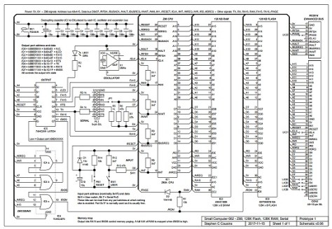
The Small Computer design 002 is a minimal Z80 system.
It has 128k bytes of FLASH and 128k bytes of RAM. A simple paging system allows access to all of the memory. A serial port is included for connection to a terminal. Expansion is available through an RC2014 bus connector.
Component count:
5 x Integrated circuits (Z80, 128k byte RAM, 128k byte FLASH, 74HCT259, 74HCT4075)
1 x Oscillator
Assorted passive components
Currently this is a paper design only and has not been tested.
View Circuit Description (PDF)
The user interface is provided by a terminal connected via the serial interface. Typically an FTDI cable will be used to connect to two.
The ROM can hold the Small Computer Monitor software, plus anything else required.
Paging allows the ROM to be removed from the memory map, under software control, and replaced by RAM. Two 64k byte RAM banks are available which can be selected under software control. A ‘page’ signal allows external devices to poke holes in the RAM address range if required.
Outputs are provided by an 8-bit addressable latch. Address line A0 provides the ‘data’ bit for the latch. This mechanism has a number of advantages over the more common 8-bit D-type flip-flop arrangement. Firstly, when only one output bit is to be controlled there is no need for the usual bit manipulation and storing a copy of the output byte in RAM. Secondly, when setting or resetting a bit no registers or flags need to be modified as the single instruction OUT (n),A can be used (where the value of ‘A’ is irrelevant).
Inputs are achieved by feeding signals to the data bus via resistors. If no other device is driving the data bus, the bus logic level is determined by the inputs. This is a bit of a dirty trick and has the disadvantage of loading the bus, but it is simple and cheap. You can only use the trick once on each bus signal.
