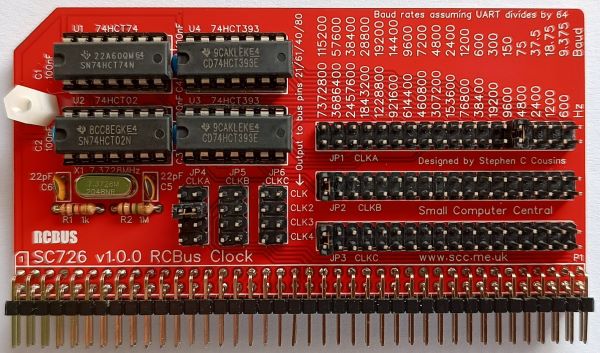
SC726 is a triple output clock generator designed for the RCBus. It provides a wide range of clock signals that can be output to various bus pins. Typically, these are used as the CPU clock and/or serial port baud rate clocks.
- SC726 – Assembly guide
- SC726 – Compatibility
- SC726 – Parts list
- SC726 – Printed circuit board
- SC726 – User guide
- SC700 series information
- SC700 series support
Downloads
- SC726 v1.0, Kit contents sheet (PDF)
- SC726, v1.0, Schematic (PDF)
- SC726, v1.0, PCB design files (OSHWLab)
- SC726, v1.0, Gerber files (ZIP)
Errata
- Nothing known
Suppliers
| Kits | Website | From | Currency |
| Small Computers Direct | SCDirect | UK | GBP |
| Stephen C Cousins | Tindie | UK | USD |
| Small Computer Central | Lectronz | UK | Euro/USD |
| PCBs | Website | From | Currency |
| Small Computers Direct | SCDirect | UK | GBP |
| Stephen C Cousins | Tindie | UK | USD |
| Small Computer Central | Lectronz | UK | Euro/USD |
| Assembled and Tested | Website | From | Currency |
| Not available | |||
| Components | |||
| See parts list |
Tindie does not collect VAT for EU countries
Lectronz does collect EU VAT for orders up to 150 EUR
Parts List
| Reference | Qty | Component |
| PCB | 1 | SC726, v1.0, PCB |
| C1 to C4 | 4 | Capacitor, ceramic, 100 nF |
| C5 and C6 | 2 | Capacitor, ceramic, 22 pF |
| JP1 to JP3 | 3 | Header, male, 2 row x 18 pin, straight |
| JP4 to JP6 | 3 | Header, male, 2 row x 4 pin, straight |
| Jumper | 6 | Jumper shunt |
| P1 | 1 | Header, male, 2 row x 40 pin, angled |
| R1 | 1 | Resistor, 1k, 0.25W |
| R2 | 1 | Resistor, 1M, 0.25W |
| Screw (for spacer) | 1 | Machine screw, 6mm, M3 |
| Spacer | 1 | Spacer, 10mm, M3, nylon |
| U1 | 1 | 74HCT74 |
| U2 | 1 | 74HCT02 |
| U3 and U4 | 2 | 74HCT393 |
| X1 | 1 | Crystal, 7.3728 MHz |
| IC socket 14-pin U1 to U4 | 4 | Socket, DIP, 14-pin |
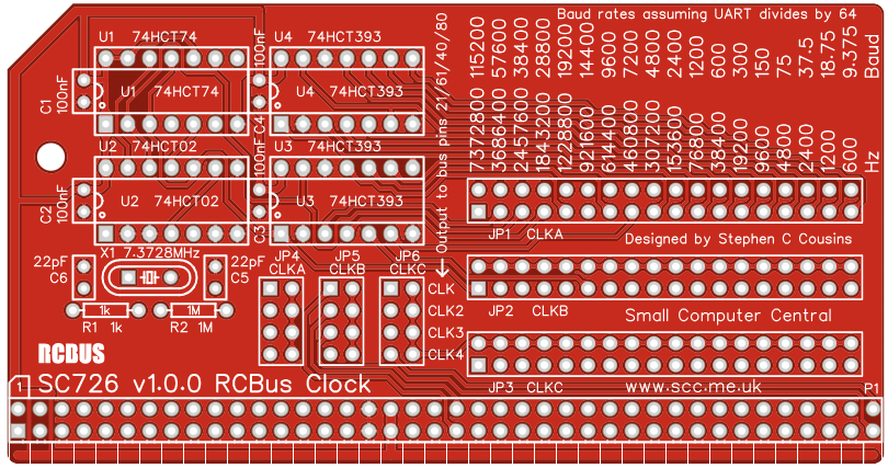
Printed Circuit Board
The printed circuit board has the dimensions recommended in the RCBus specification for a medium sized module.
User Guide
SC726 is clock signal generator designed for the RCBus. It provides a wide range of cock frequencies which can be connected to various pins on the RCBus, including the main CPU clock (CLK), the second bus clock (CLK2) and two user pins (USER4 and USER8). The second bus clock is usually used as a baud rate clock for serial modules.
Only one clock source should be connected to any given pin. As some modules include a CPU clock (CLK) and some a second bus clock (CLK2), care must be taken to not connect a second source to these pins. Most modules that provide these signals have jumpers to isolate them, thus allowing a dedicated clock module, such as SC726, to provide these signals.
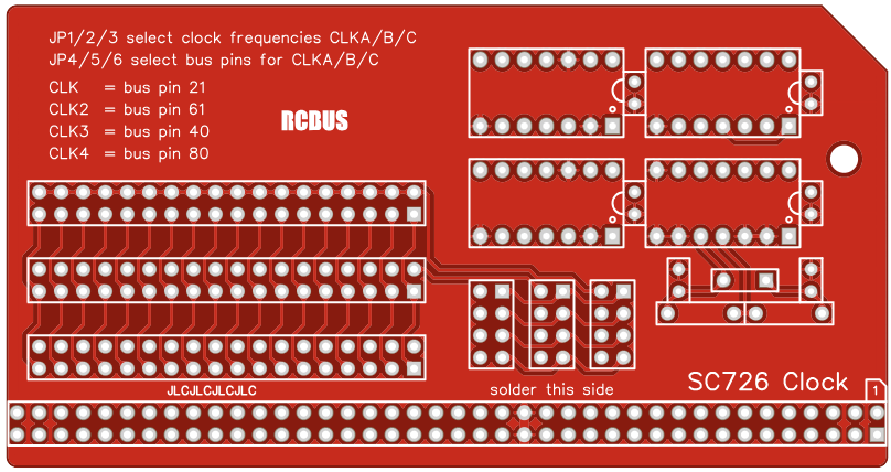
The module provides three clock signals (CLKA, CLKB and CLKC). The frequency of each of these signals is set with JP1, JP2 and JP3 respectively. Each of these three clock signals can be connected to any of the four destinations (pin 21 CLK, pin 61 CLK2, pin 40 USER4 and pin 80 USER8) with JP4, JP5 and JP6.
When used as baud rate clocks for serial ports the clock is normally divided by 16 or 64 in the serial IC to give the baud rate. The silk screen shows baud rates assuming the serial IC divides the clock by 64.
Input/output port functions
| RCBus I/O Address | Read | Write |
| none | n/a | n/a |
Jumper options
| Jumper | Function |
| JP 1 | Select CLKA frequency The default is 7372800 Hz |
| JP 2 | Select CLKB frequency The default is 7372800 Hz |
| JP 3 | Select CLKC frequency The default is 7372800 Hz |
| JP 4 | Select destination for CLKA JP 4.1 Connect CLKA to RCBus pins 21 (CLK) JP 4.2 Connect CLKA to RCBus pins 61 (CLK2) JP 4.3 Connect CLKA to RCBus pins 40 (USER4) JP 4.4 Connect CLKA to RCBus pins 80 (USER8) The default is jumper shunt not fitted |
| JP 5 | Select destination for CLKB JP 4.1 Connect CLKB to RCBus pins 21 (CLK) JP 4.2 Connect CLKB to RCBus pins 61 (CLK2) JP 4.3 Connect CLKB to RCBus pins 40 (USER4) JP 4.4 Connect CLKB to RCBus pins 80 (USER8) The default is jumper shunt not fitted |
| JP 6 | Select destination for CLKC JP 4.1 Connect CLKC to RCBus pins 21 (CLK) JP 4.2 Connect CLKC to RCBus pins 61 (CLK2) JP 4.3 Connect CLKC to RCBus pins 40 (USER4) JP 4.4 Connect CLKC to RCBus pins 80 (USER8) The default is jumper shunt not fitted |
Assembly Guide
Below is the suggested order of assembly. A general guide to assembling circuit boards can be found here.
- Resistors R1 and R2
These can be fitted either way around - Decoupling capacitors C1 to C4
These can be fitted either way around - Capacitors C5 and C6
These can be fitted either way around - Sockets for U1 to U4
Fit such that the notch in the socket matches the curve in the outline on the PCB silkscreen - Bus header P1
Make sure the pins are parallel to the PCB so that the board is vertical when it is fitted into a backplane socket - Header pins JP1 to JP6
- Crystal X1
This can be fitted either way around - Insert the integrated circuits into their sockets
Make sure the notch in the component is at the end indicated by the notch in the socket and the curve on the PCB silkscreen - Fit the nylon spacer in the mounting hole
Fit jumper shunts in the positions shown below. All other jumpers are optional and should only be fitted if the feature is required.

Compatibility
This module conforms fully to the RCBus specification v1.0 and thus supports: RCBus-2014, RCBus-Z80, RCBus-68xx, RCBus-9995.
The RCBus specification includes RCBus-2014 (both RC2014 standard 40-pin bus and RC2014 enhanced 60-pin bus) and also the full 80-pin RCBus. The 80-pin RCBus provides support for advanced Z80 features, such as the interrupt daisy-chain, as well as support for other processor families.
The table below indicates electrical compatibility with each backplane type (40, 60 and 80 pin)

| Backplane | ? | Compatibility notes |
| RCBus 80-pin |  | Fully supported |
| RCBus 60-pin (RC2014 enhanced) | | Limitations: Optional signal CLK4 not usually available |
| RCBus 40-pin (RC2014 standard) | | Limitations: Some optional signals are not available (CLK2, CLK4) |
Notes
- This product is designed for hobby use and is not suitable for industrial, commercial, or safety-critical applications.
- The product contains small parts and is not suitable for young children.
