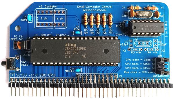
SC153 is a Z80 Central Processor Unit (CPU) module with three clock oscillator options, and an optional voltage supervisor and reset device, designed for the RC2014 bus.
A later design is now available: SC706
- SC153 – Assembly Guide
- SC153 – Parts List
- SC153 – Printed Circuit Board
- SC153 – Support
- SC153 – User Guide
Downloads
- SC153, v1.1, Kit contents sheet (PDF)
- SC153, v1.1, Schematic (PDF)
- SC153, v1.1, PCB design files (OSHWLab)
- SC153, v1.1, Gerber files (ZIP)
Errata
- PCB SC153 v1.1.0 needs a wire link for capacitor C7 if the oscillator X2 is not populated
Suppliers
| Kits | Website | From | Currency |
| Small Computers Direct | SCDirect | UK | GBP |
| Stephen C Cousins | Tindie | UK | USD |
| Small Computer Central | Lectronz | UK | Euro/USD |
| PCBs | Website | From | Currency |
| Small Computers Direct | SCDirect | UK | GBP |
| Stephen C Cousins | Tindie | UK | USD |
| Small Computer Central | Lectronz | UK | Euro/USD |
| Assembled and Tested | Website | From | Currency |
| Not available | |||
| Components | |||
| See parts list |
Tindie does not collect VAT for EU countries
Lectronz does collect EU VAT for orders up to 150 EUR
Parts List
| Reference | Qty | Component |
| PCB | 1 | SC153, v1.1, PCB |
| C1 to C4 | 4 | Capacitor, ceramic, 100 nF |
| C5and C6 | 2 | Capacitor, ceramic, 22 pF |
| C7 and C8 | 0 | Capacitor, ceramic, ~22 pF Not included in the kit Fit a wire link at C7 |
| C9 | 1 | Capacitor, ceramic, 1 nF |
| JP1 | 1 | Header, male, 2 row x 4 pin, straight or male, 2 row x 4 pin, angled Straight pins included in kit |
| Jumper | 2 | Jumper shunt |
| P1 | 1 | Header, male, 2 row x 40 pin, angled (some pins need to be removed) |
| P2 | 0 | Typically header, male, 1 row x 2 pin Not included in the kit |
| R1 | 1 | Resistor, 1M, 0.25W |
| R2 | 1 | Resistor, 1k, 0.25W |
| R3 | 0 | Resistor, ~1M, 0.25W Not included in the kit |
| R4 | 0 | Resistor, ~1k, 0.25W Not included in the kit |
| R5 to R9 | 5 | Resistor, 10k, 0.25W |
| SW1 | 1 | Switch, tactile button, angled |
| U1 | 1 | Z80 CPU, Z84C0008PEG, or Z80 CPU, Z84C0010PEG |
| U2 | 1 | 74HCT04 |
| U3 | 1 | DS1233-5+ supervisor |
| X1 | 1 | Crystal, 7.3728MHz |
| X2 | 0 | Crystal, typically 2 to 10MHz Not included in the kit |
| X3 | 0 | Oscillator, 8 or 14-pin Not included in the kit |
| IC socket 40-pin U1 | 1 | Socket, DIP, 40 pin |
| IC socket 14-pin U2 | 1 | Socket, DIP, 14-pin |
Printed Circuit Board
User Guide
SC153 provides a Z80 Central Processor Unit (CPU) module with three clock oscillator options, and an optional voltage supervisor and reset device, designed for the RC2014 bus.
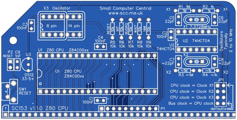
The PCB has three clock oscillators, with the required oscillator selected with a jumper. This allows several different oscillators to be including with easy selection of the desired clock source. The kit includes parts for clock oscillator 1 only (7.3728 MHz). If X2 is not populated, solder a link across C7 so the input to U2 is not left floating. Strange things can happen if it is left floating.
It is also possible to build the PCB without any of the oscillator parts and use a clock source from a different module on the bus. Alternatively, the clock source selection jumper (X1, X2 or X3) can be left off so the onboard oscillator(s) are isolated and not used. This jumper simply connects the required oscillator output to the CPU’s clock input pin.
There is also a jumper to allow the CPU’s clock to be connected to the RC2014 bus CLK signal. This is normally desirable but it can be isolated if required.
The voltage supervisor and reset device (U3) provides a reliable power up reset. It works by holding the CPU in reset until the supply voltage reaches approximately 4.75 volts. If the system does not seem to be working, always check the supply voltage is above 4.75 volts on the PCB and that the RESET signal is a logic high voltage, typically above 4 volts. The supervisor should hold the reset low of about 0.5 seconds after the system is turned on and after the reset button is released.
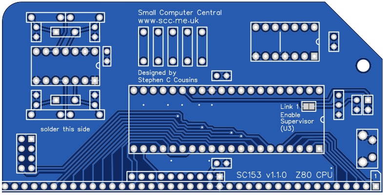
The system should only include one enabled voltage supervisor, so a solder link has been provided on the solder side of the PCB to connect or isolate this device. Normally, it should be connected, but if you have a supervisor on another module you may need to isolate this one.
Input/output port functions
| I/O Address | Read | Write |
| none | n/a | n/a |
Jumper options
| Jumper | Function |
| JP1 | Clock signals JP1.1 connects CPU clock to Clock X1 JP1.2 connects CPU clock to Clock X2 JP1.3 connects CPU clock to Clock X3 JP1.4 connects Bus clock to CPU clock |
| Link 1 | Enable voltage supervisor A solder link option on the solder side of the PCB enables the voltage supervisor to be connected |
Clock oscillators X2 and X3 are optional. The default is to connect the output of clock oscillator X1 to the CPU and the RC2014 bus CLK pin. This requires a jumper shunt in each of the two marked default positions (JP1.1 and JP1.4). If you wish to use a clock sourced from a different module then the X1 jumper should be removed.
Link 1 (a solder link on the solder side of the PCB) should be bridged with solder if the voltage supervisor is to be used. This link connects the voltage supervisor to the RESET signal. The system should only contain one enabled supervisor, thus the link has been provided to isolate or connect this device.
Assembly Guide
Below is the suggested order of assembly. A general guide to assembling circuit boards can be found here.
The kit does not include parts for the optional oscillators X2 and X3. Fit a wire link for capacitor C7 if the oscillator X2 is not populated.
- Resistors R1, R2, R5, R6, R7, R8 and R9
These can be fitted either way around - Sockets for U1 and U2
Fit such that the notch in the socket matches the curve in the outline on the PCB silkscreen - Bus header P1
Some pins need to be pulled out of the second row to match the holes in the PCB. Make sure the pins are parallel to the PCB so that the board is vertical when it is fitted into a backplane socket - Decoupling capacitors C1, C2, C3, C4, C5, C6 and C9
These can be fitted either way around - If X2 is not populated, solder a link across C7 so the input to U2 is not left floating. Strange things can happen if it is left floating.
- Header pins JP1
Fit a jumper shunts in the default “CPU clock = Clock X1” and “Bus clock = CPU clock” positions of JP1, as indicated on the PCB - Crystal X1
These can be fitted either way around - Switch SW1
- Voltage supervisor U3
Carefully bend the legs to match the hole spacing on the PCB and ensure the orientation matches the markings on the PCB - Connect link 1 on the solder side of the PCB by bridging with solder, but only if you want to connect the voltage supervisor and reset device
- Insert the integrated circuits into their sockets
Make sure the notch in the component is at the end indicated by the notch in the socket and the curve on the PCB silkscreen
Notes
- This design is made in accordance with the “designed for RC2014” labelling scheme.
- RC2014 is a trademark of RFC2795 Ltd.
- This product is designed for hobby use and is not suitable for industrial, commercial, or safety-critical applications.
- The product contains small parts and is not suitable for young children.
