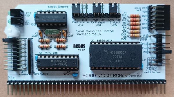
SC610 is a serial port module for the 40-pin RCBus.
A comparison of serial modules can be found here.
- SC610 – Assembly guide
- SC610 – Compatibility
- SC610 – Parts list
- SC610 – Printed circuit board
- SC610 – User guide
- SC600 series information
- SC600 series support
Downloads
- SC610, v1.0, Kit contents sheet (PDF)
- SC610, v1.0, Schematic (PDF)
- SC610, v1.0, PCB design files (OSHWLab)
- SC610, v1.0, Gerber files (ZIP)
Errata
Nothing known
Suppliers
| Kits | Website | From | Currency |
| Small Computers Direct | SCDirect | UK | GBP |
| Stephen C Cousins | Tindie | UK | USD |
| Small Computer Central | Lectronz | UK | Euro/USD |
| PCBs | Website | From | Currency |
| Small Computers Direct | SCDirect | UK | GBP |
| Stephen C Cousins | Tindie | UK | USD |
| Small Computer Central | Lectronz | UK | Euro/USD |
| Assembled and Tested | Website | From | Currency |
| Not available | |||
| Components | |||
| See parts list |
Tindie does not collect VAT for EU countries
Lectronz does collect EU VAT for orders up to 150 EUR
Parts List
| Reference | Qty | Component |
| PCB | 1 | SC610, v1.0, PCB |
| C1 to C4 | 4 | Capacitor, ceramic, 100 nF |
| C5 and C6 | 2 | Capacitor, ceramic, 22 pF |
| JP1 | 1 | Header, male, 2 row x 8 pin, angled or straight ? |
| JP2+3+7+8 | 1 | Header, male, 2 row x 8 pin, angled Some pins need to be removed |
| JP4+5+6 | 1 | Header, male, 1 row x 12 pin, angled Some pins need to be removed |
| Jumper | 14 | Jumper shunt |
| LED1 and 2 | 2 | LED, green, 3mm, angled |
| P1 | 1 | Header, male, 1 row x 40 pin, angled |
| P2 | 1 | Header, male, 1 row x 6 pin, angled |
| R1 to R4 | 4 | Resistor, 2k2, 0.25W |
| R5 and R6 | 2 | Resistor, 100k, 0.25W |
| R7 | 1 | Resistor, 1M, 0.25W |
| R8 to R10 | 3 | Resistor, 1k, 0.25W |
| RP1 | 1 | Resistor network, 8x100k, SIL, 9-pin |
| S1 | 1 | Header, female, 1 row x 6 pin, angled |
| Screw (for spacer) | 1 | Machine screw, 6mm, M3 |
| Spacer | 1 | Spacer, 10mm, M3, nylon |
| U1 | 1 | 74HCT688 |
| U2 | 1 | 68B50 ACIA |
| U3 | 1 | 74HCT04 |
| X1 | 1 | Crystal, 7.3728 MHz |
| IC socket 20-pin U1 | 1 | Socket, DIP, 20-pin |
| IC socket 24-pin U2 | 3 | Socket, DIP, 24-pin |
| IC socket 14-pin U3 | 1 | Socket, DIP, 14-pin |
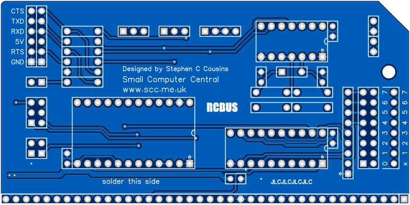
Printed Circuit Board
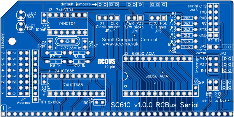
Note: The PCB is designed to allow a DIP switch to be fitted instead of the header pins JP1.
User Guide
The serial port provides bidirectional asynchronous serial communications usually at 115200 baud, 8 data bits, 1 stop bit, no parity. RTS/CTS handshaking provides hardware flow control in both directions. The interface is at 5-volt (TTL) levels.
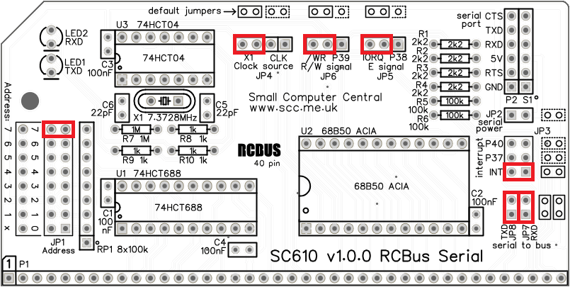
The RCBus I/O port address for this module is set in binary with JP1. Fit a jumper shunt to each bit position where the address bit should be a logic ‘1’ (high voltage).
The default address is 128 decimal, which is 0x80 in hexadecimal and 1000000 in binary. To set this as the address requires a jumper shunt in bit position 8, as illustrated below.
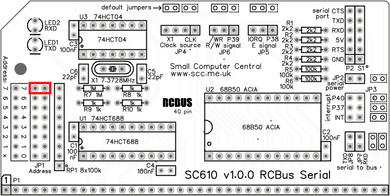
The module occupies two addresses so bit zero of the address can be in either state. The address jumper bit zero is labelled ‘x’ to indicate this.
Jumper JP2 connects the module’s 5-volt supply to the serial port. A jumper should should be fitted here if the RCBus system is being powered from this serial port or if the device connected to this serial port needs to be powered from the RCBus system.
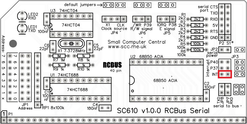
Jumper JP3 enables the ACIA’s interrupt output to be connected to the bus signals INT, INT1 (bus pin 37) or INT2 (bus pin 40). The default position is INT.
Jumper JP4 enables selection of the clock source for the ACIA. This can either be the on-board 7.3728 MHz oscillator or the RCBus clock signal (CLK). Selecting the on-board clock means the serial port baud rate is independent of the processor speed.
It is also possible to use the onboard oscillator as the main bus clock by fitting jumper shunts to both the X1 and the CLK positions of JP4. Take care to only have one clock source connected to the main bus clock signal (CLK).
JP5 and JP6 enable selection of the ACIA’s R/W and E inputs. Normally these are set to the IORQ and WR signals that are common to all implementations of the RCBus. Alternative, if the processor supports native R/W and E signals then these can be selected instead.

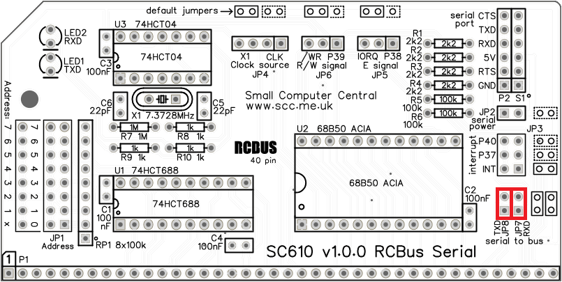
JP7 and JP8 enable the ACIA’s RXD and TXD signals to be connected to the RCBus RX and TX pins as illustrated below.
Input/output port functions
| RCBus I/O Address | Read | Write |
| Configurable *1 | Read ACIA | Write ACIA |
| base + 0 | Status register | Control register |
| base + 1 | Receive data register | Transmit data register |
- The RCBus I/O address should be set to match the software you are using. Typically, this is 0x80 or 0x40.
Jumper options
| Jumper | Function |
| JP 1 | Set SC610’s RCBus I/O address |
| JP 2 | Connects 5-volt power to serial port |
| JP 3 | Selects which interrupt signal is generated JP 3.1 Interrupt goes to RCBus INT signal JP 3.2 Interrupt goes to RCBus INT1 signal JP 3.3 Interrupt goes to RCBus INT2 signal The default is INT |
| JP 4 | Select the clock source JP 4.1-2 Clock source is the RCBus CLOCK signal JP 4.3-4 On-board 7.2728 MHz oscillator If jumper shunts are fitted in both positions the on-board oscillator supplies the RCBus CLOCK signal The default is the on-board oscillator |
| JP 5 | Select the E signal source JP 5.1-2 RCBus pin 38 (for use with 68xx processors) JP 5.2-3 RCBus nIORQ (inverted) The default is the inverted nIORQ signal |
| JP 6 | Selects to R/W signal source JP 6.1-2 RCBus pin 39 (for use with 68xx processors) JP 6.2-3 RCBus nWR signal The default is the nWR signal |
| JP 7 | Connects the RXD input and the CTS input to the bus JP 7.1-2 Connects RXD to bus RX signal |
| JP 8 | Connects the TXD output and the RTS output to the bus JP 8.1-2 Connects TXD to bus TX signal |
Assembly Guide
Below is the suggested order of assembly. A general guide to assembling circuit boards can be found here.
- Resistors R1 to R10
- Socket S1
- Decoupling capacitors C1 to C4 (100 nF)
These can be fitted either way around - Bus header pins P1
- Header pins JP4, JP5 and JP6
Fit as one strip with pins 4 and 8 removed - Serial header pins P2
- Crystal X1
- IC sockets for U1 to U3
Ensure the notch in the socket matches the marking on the PCB - Capacitors C5 and C6 (22 pF)
These can be fitted either way around - Resistor network RP1 (8 x 100k)
- Header pins JP1
You may wish to remove the pins for address bit zero as the module occupies two I/O addresses and therefore bit zero is not used - Header pins JP2, JP3, JP7 and JP8
Fit as one strip with pins 2 and 6 removed - LED1 and LED2
The angled LEDs in the kit only fit one way around, but standard LEDs need to have the short lead in the hole marked with a flat line - Fit the IC’s in their sockets
Ensure the notch in the IC matches the PCB and IC socket - Fit the nylon spacer in the mounting hole
Fit jumper shunts in the positions shown below.
Compatibility
This module conforms to the RCBus specification v1.0 for RCBus-2014 (40-pin bus) and RCBus-Z80 (40-pin bus).
The RCBus specification includes RCBus-2014 (both RC2014 standard 40-pin bus and RC2014 enhanced 60-pin bus) and also the full 80-pin RCBus. The 80-pin RCBus provides support for advanced Z80 features, such as the interrupt daisy-chain, as well as support for other processor families.
The table below indicates electrical compatibility with each backplane type (40, 60 and 80 pin)

| Backplane | ? | Compatibility notes |
| RCBus 80-pin |  | Fully supported |
| RCBus 60-pin (RC2014 enhanced) | | Fully supported |
| RCBus 40-pin (RC2014 standard) | | Fully supported |
Notes
- This product is designed for hobby use and is not suitable for industrial, commercial, or safety-critical applications.
- The product contains small parts and is not suitable for young children.
