SC103 is a very flexible Z80 PIO module designed for the RC2014 bus.
A later design is now available: SC717

Documentation
- SC103 – Assembly guide
- SC103 – Circuit explained
- SC103 – Parts list
- SC103 – Printed circuit board
- SC103 – User guide
- SC103 – PCB design files v1.1 (EasyEDA)
Downloads
Suppliers
| Kits | Website | From | Currency |
| Small Computers Direct | SCDirect | UK | GBP |
| Stephen C Cousins | Tindie | UK | USD |
| Small Computer Central | Lectronz | UK | Euro/USD |
| PCBs | Website | From | Currency |
| Small Computers Direct | SCDirect | UK | GBP |
| Stephen C Cousins | Tindie | UK | USD |
| Small Computer Central | Lectronz | UK | Euro/USD |
| Assembled and Tested | Website | From | Currency |
| Not available | |||
| Components | |||
| See parts list |
Tindie does not collect VAT for EU countries
Lectronz does collect EU VAT for orders up to 150 EUR
Examples
Older Versions
Description
The final installment in my set of three Z80 peripheral chip modules designed for RC2014.
This module houses a Z80 PIO chip and provides two 8-bit I/O ports with handshaking.

The main features of this module are:
- Full Z80 mode 2 interrupt support (IEI/IEO daisy-chain)
- Tight address decoding
- DIP switch address selection
- Two 8-bit I/O ports with handshaking
- Connector on rear edge for ribbon cable
- Connector on top edge suitable for Dupont cable
My first application of the PIO module application is a simple alphanumeric LCD interface.

User Guide
The Z80 PIO module (SC103) provides two 8-bit parallel ports with handshaking and flexible input and output connectivity, as well as support for Z80 mode 2 interrupt daisy chaining.

Each port has eight bidirectional data lines and two handshaking lines. The PIO has flexible interrupt generation and fully supports Z80 mode 2 interrupts.
For full details of the Z80 PIO see the Zilog data sheet.
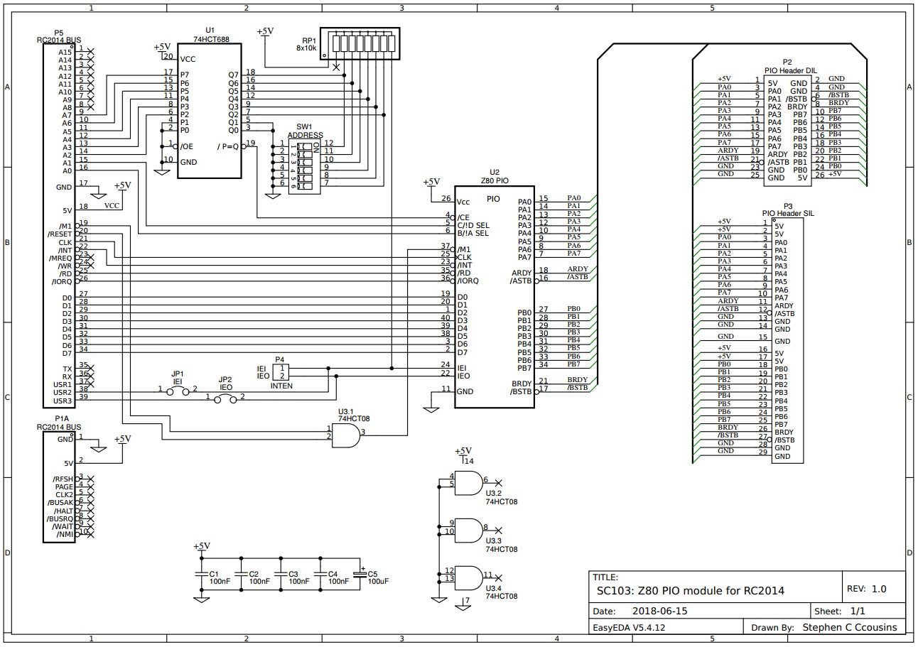
Schematic
Errata
Version 1.0 of the PCB has the RC2014 IEI (pin 38) and IEO (pin 39) incorrectly labelled. The labels are incorrectly shown next to pins 37 and 38, not 38 and 39.
Version 1.0 of the PCB has port A I/O lines incorrectly labelled on the back of the board. The labels on the front of the board are correct though.
Configuring the Module
The only jumpers on the PIO board are for interrupt daisy chain signals IEI and IEO. If your system has more than one device using interrupt mode 2, it will be necessary to set up an interrupt daisy chain.
This is fully described in the Z80 peripherals data sheet, but essentially it requires linking the output (IEO) of one interrupt generating device to the input (IEI) of the next, and so on. The position in the chain determines the device’s interrupt priority.
The illustration shows the connections required when using external Dupont wires on P4 (shown in red) and the RC2014 bus USER pins (shown in yellow). To connect the IEI and IEO signals to the RC2014 bus fit shunts to jumpers J1 and J2 (shown in green).
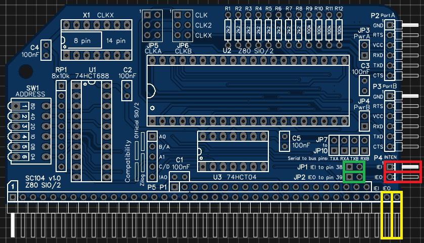
Note that v1.0 of the PCB has the IEI and IEO bus pins incorrectly labelled. It indicates the use of pins 37 and 38, not 38 and 39.
Setting up a mode 2 interrupt system is not trivial so requires study of the data sheets rather than following any simple example I could write here.
Address Selection
The module’s address can be set to any address that is a multiple of 4, such as address 0, 4, 8, 12, 16, … , 252. This address is known as the base address, with the module occupying this address plus the next three addresses. Thus if the base address is 0, then the module occupies the address range 0 to 3.
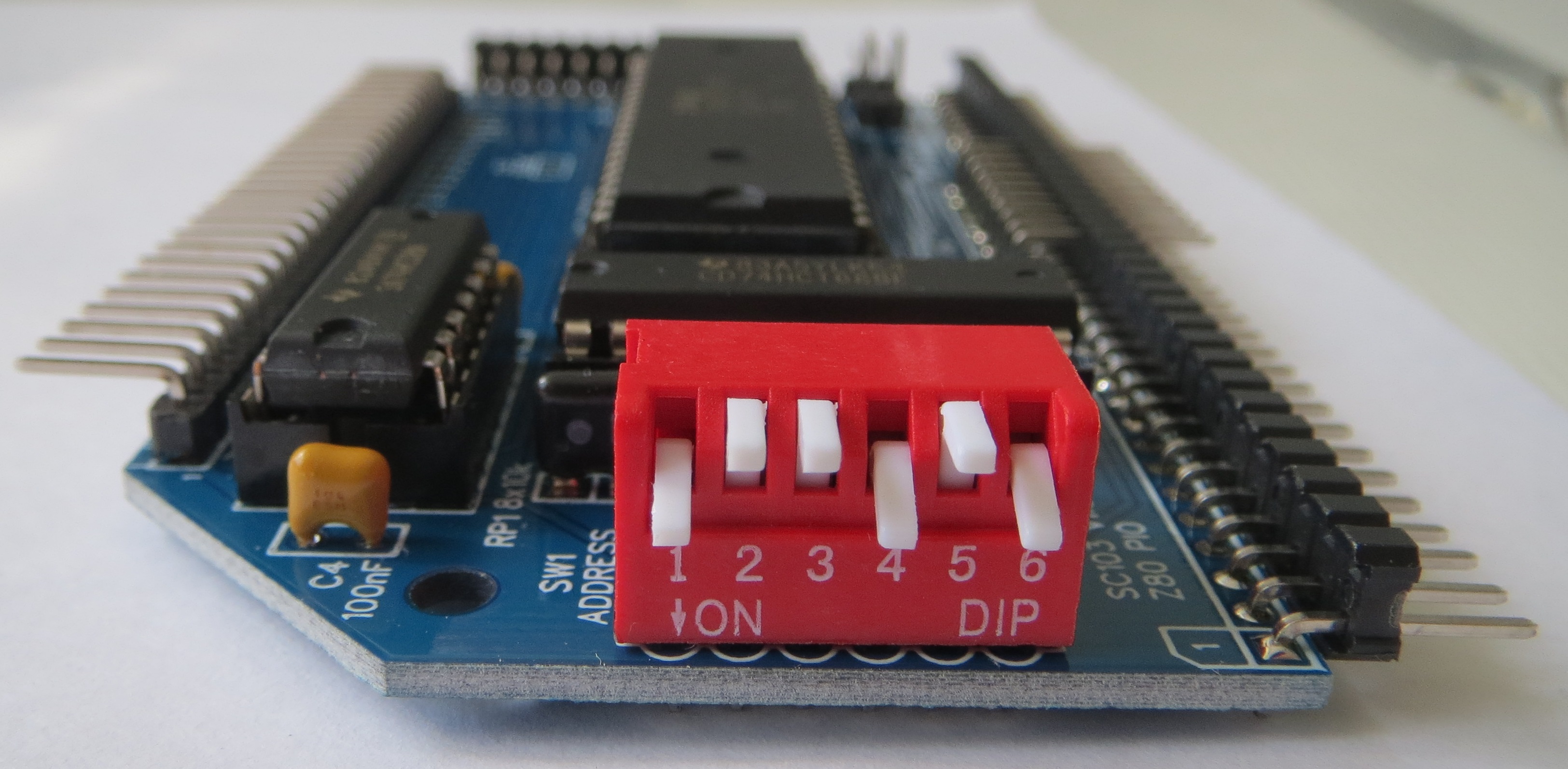
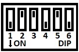
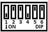
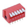
The address is set with the 6 way DIP switch SW1.
The six address switches, 1 to 6, represent addresses 128, 64, 32, 16, 8 and 4 respectively. The base address is the sum of all the switches in the Off position. For a piano style DIP switch, as illustrated below, Up is Off and Down is On.
In the illustration below the switches are:
Down Up Up Down Up Down
This represents the address:
0 + 64 + 32 + 0 + 8 + 0
= 64 + 32 + 8
= 104 (or 0x68 in hexadecimal).
In order to provide some certainty for software it is recommended you set the base address of your first PIO module to 0x68, so that the module occupies I/O addresses 0x68 to 0x6B. This is done by setting the switches as illustrated above.
If you have a second PIO module the recommended base address is 0x6C.
If everybody follows theses recommendations then software written for the PIO module will know where to find the PIO hardware.
The following table shows examples of address switch settings.
Switch
Address
Recommended 1st PIO
Base address 0x68
Range 0x68 to 0x6B
(104 to 107 decimal)
Recommended 2nd PIO
Base address 0x6C
Range 0x6C to 0x6F
(108 to 111 decimal)
Base address 0x00
Range 0x00 to 0x03
(0 to 3 decimal)

Base address 0x04
Range 0x04 to 0x07
(4 to 7 decimal)

Base address 0x08
Range 0x08 to 0x0B
(8 to 11 decimal)

Base address 0x40
Range 0x40 to 0x43
(64 to 67 decimal)

Base address 0x44
Range 0x44 to 0x47
(68 to 71 decimal)

Base address 0x48
Range 0x48 to 0x4B
(72 to 75 decimal)

Base address 0x4C
Range 0x4C to 0x4F
(76 to 79 decimal)

Base address 0x50
Range 0x50 to 0x53
(80 to 83 decimal)

Base address 0xF0
Range 0xF0 to 0xF3
(240 to 243 decimal)

Base address 0xF4
Range 0xF4 to 0xF7
(244 to 247 decimal)
Base address 0xF8
Range 0xF8 to 0xFB
(248 to 251 decimal)
Base address 0xFC
Range 0xFC to 0xFF
(252 to 255 decimal)
Credits
Thanks to all those who provided encouragement, feedback and contributed ideas to the design. Specifically: Mark T, Jon L, Jay C, and anyone else I forgot!
See RC2014 google group for full details:
https://groups.google.com/forum/#!topic/rc2014-z80/JJ2JKAIehck
Parts List
| Reference | Qty | Component |
| PCB | 1 | SC103, v1.0, PCB |
| C1 to C4 | 4 | Capacitor, ceramic, 100 nF |
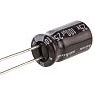
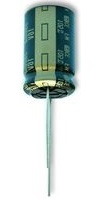
| C5 | 1 | Capacitor, electrolytic, 100 µF |
| JP1 plus JP2 | 1 | Header, male, 2 x 2 pin, straight |
| JP1 and JP2 shunt | 2 | Jumper shunt |
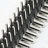
| P1 | 1 | Header, male, 2 x 39 pin, angled |
| P2 | 1 | Header, male, 2 x 13 pin, angled |
| P3 | 1 | Header, male, 1 x 29 pin, angled |
| P4 | 1 | Header, male, 1 x 2 pin, angled |
| RP1 | 1 | Resistor pack, 8 x 10k, SIL, 9-pin |
| SW1 | 1 | DIP switch, 6 way, piano style |
| U1 | 1 | 74HCT688 |
| U1 socket | 1 | 20-pin DIP socket |
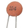
| U2 | 1 | Z80 PIO, Z84C2008PEG |
| U2 socket | 1 | 40-pin DIP socket |
| U3 | 1 | 74HCT08 |
| U3 socket | 1 | 14-pin DIP socket |
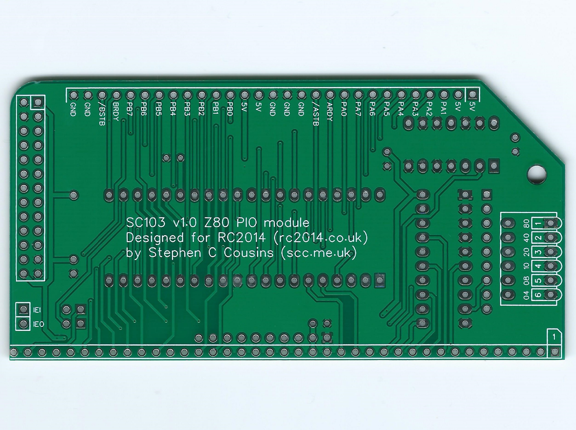
Printed Circuit Board
PCB v1.1 fixes the errors on some pin labels of PCB v1.0. The tracks have not changed and thus schematic v1.0 is still correct for PCB v1.1.

| Supplier | Website | Ships from |
| Stephen C Cousins | Tindie | UK |
| pcb4diy | eBay | Germany |
| pcb4diy | pcb4diy.de | Germany |
Assembly Guide
Experienced builders can just go ahead and populate the board. There shouldn’t be any surprises to catch you out.
This guide assumes you are familiar with assembling circuit boards, soldering, and cleaning. If not, it is recommended you read some of the guides on the internet before continuing.
First check you have all the required components.
Before assembling it is worth visually inspecting the circuit board for anything that looks out of place, such as mechanical damage or apparent manufacturing defects.
If you have a multimeter that measures resistance or has a continuity test function, check there is not a short on the power supply tracks. Connect the probes to each terminal of one of the capacitors, such as C1. This should be an open circuit, not a short.
The picture below shows what a completed SC103 Z80 PIO Module should look like.
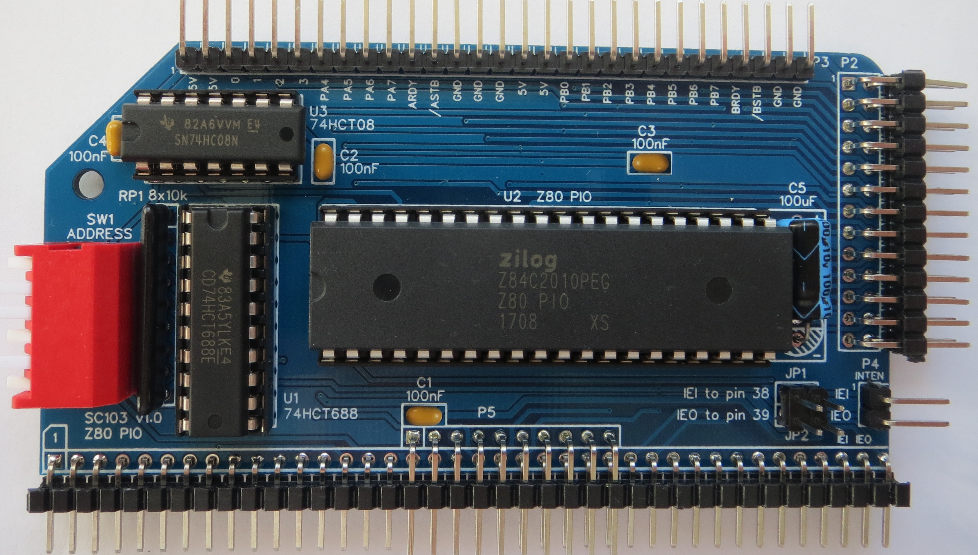
IC sockets
Fit and solder IC sockets for U1, U2, and U3.
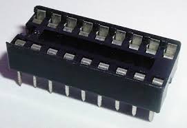
Be sure to fit them with the notch matching the legend on the circuit board, so you do not end up fitting the IC the wrong way round too.
The sockets should be fitted in the positions shown below.

Capacitors
Fit and solder capacitors C1 to C4.
These can be fitted either way round, as they are not polarity dependent.

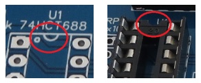
Resistor Network
Fit and solder the 8x10k resistor network.

This must be fitted the correct way round. The component should have pin 1 marked with a dot, as illustrated right.


Bus Connector
Fit and solder bus connector P1.

You can fit just a single row header, as used by the RC2014 Standard bus, if you wish.
To prepare the header, it should first be cut to length (if starting with a strip more than 39 pins long) and then unwanted pins must be removed. If you want to make the board as easy to insert and remove as possible, you can remove all the pins in the second row except those shown on the schematic as used and indicated below in green.

Take care to ensure the pins are parallel to the circuit board so that the board will be vertical when plugged into a backplane.

Header Pins P2
Fit and solder the
double row right-angled male header pins P2.
Take care to ensure the header pins are parallel to the circuit board.

Header Pins P3
Fit and solder the right-angled male header pins, P3.
Take care to ensure the pins are parallel to the circuit board.
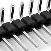

Header Pins P4
Fit and solder the right-angled male header pins, P4.
Take care to ensure the pins are parallel to the circuit board.


Jumper Pins
Fit and solder the jumper pins for JP1 and JP2.
JP1 and JP2 are combined as a single, 2 row by 2 pin header.


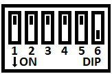
Address Select Switch
Fit and solder the 6-way DIP switch SW1.
Take care not to overheat this component when soldering.

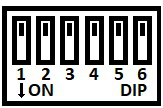
Address Select Switch
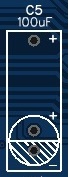
The PCB allows for a radial or axial capacitor. In order to build a low profile board, the capacitor should lay on its side. An axial capacitor would be most secure in this configuration, but there is limited length allocated and you probably don’t have one!
You can fit a radial capacitor on its side, but it is not as secure as an axial package as both leads come out of the same end.
It is important to fit this capacitor the right way round.
The PCB’s legend shows a plus and minus signs next to the round outline of a radial packaged capacitor, as illustrated to the right. It also shows the alternative plus position for an axial capacitor (at the top of the rectangular area). In both cases the negative terminal is at the bottom.
The images to the right show the typical markings of the negative terminal of the capacitor.

Inspection
Remove any solder ‘splats’ with a brush, such as an old toothbrush.
Visually inspect the soldering for dry joints and shorts.
Clean the flux off with suitable cleaning materials.
Visually inspect again.
Before fitting the ICs, plug the board into an RC2014 backplane with no other boards fitted. Power the backplane and perform the following checks with a voltmeter:
- Check the supply voltage on the PIO module, between, say, U1 pin 10 and U1 pin 20. This should be 4.5 to 5.5 volts, preferably 4.75 to 5.25 volts.
- Check the interrupt enable input (IEI) on connector P4 is being pulled up to at least 4.5 volts.
- Check each address switch input (Q2 to Q7) on U1 is being pulled up to at least 4.5 volts when the appropriate switch (SW1) is Off (open) and drops to less than 0.4 volts when the appropriate switch (SW1) is On (closed).
If all is well, power down and remove the PIO module.
Integrated Circuits
Insert the ICs into their sockets, taking care to insert them the correct way round, as illustrated below. Be careful not to bend any legs over.

Test
There is no need to fit any of the jumper shunts yet.
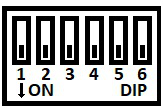
Set the DIP switches as shown below. This sets the address to the range 0x68 to 0x6B.

Now plug the PIO module into the RC2014 backplane together with your normal working set of modules. Power up and check the system is working as usual.
Details of how to use this module can be found in the SC103 Z80 PIO User Guide.
Circuit Explained
This RC2014 compatible module contains a Z80 PIO (parallel input output) chip and is designed to be very flexible, with full access to the PIO’s hardware functions via header pins.
Address Decoding
The PIO is an I/O devices occupying a block of 4 I/O addresses. The base address of this block is set with DIP switches. These allow selection of any I/O address on a 4 byte boundary.
C1 to C4
These capacitors provide power supply decoupling (or bypass). The fast switching in digital circuits creates spikes on the power supply lines which are suppressed with decoupling capacitors placed at key points on the circuit board.
C5
This capacitor provides suppression of transients on the power supply. The PIO module may well be used to power and control external electronics, in which case there could be significant transients generated on the supply lines. Where possible supply transients should be suppressed at source, so this component should not be critical.
The PCB allows for a radial or axial capacitors. In order to build a low profile board, the capacitor should lay on its side. An axial capacitor would be most secure in this configuration, but there is limited length allocated and you probably don’t have one!
JP1 and JP2
This pair of jumpers allow the interrupt daisy chain signals to be connected to the RC2014 bus signal USER 2 (pin 38) and USER 3 (pin 39). To make use of this feature you must use a backplane that is specifically designed to provide the necessary daisy chain, such as Backplane SC107. The current official RC2014 backplanes do not support this feature.
Alternatively the signals IEI and IEO can be found on connector P4 on the back edge of the board. Dupont wires can be used to daisy chain these signals to other modules.
P1
This connector mates with the RC2014 bus backplane. You can fit a single or a double row header. The only reasons for the second row is to provide additional power supply pins, make the module the same height as the others and to increase stability of the module.
P2
This connector provides access to all the PIO I/O signals in a format suitable to connect to external devices via a ribbon cable. See schematic for pin-out.
P3
This connector provides access to all the PIO I/O signals in a format suitable to connect to breadboards and other prototyping projects via Dupont wires.
This connector is optional, so if you want to put the RC2014 in a case or just don’t like the look of it, you can leave this connector off. Alternatively you might prefer a different connector, such as a female header socket.
Pin 15 is a ground terminal between the two port I/O connections. You may wish to remove this pin before assembly, so that it is easier to visually identify required connections. See schematic for pin-out.
P4
As the official RC2014 backplanes do not provide a Z80 mode 2 interrupt daisy chain (IEI and IEO signals), these have been brought to the back of the board where they can be easily linked to other modules with Dupont wires.
RP1
This is a network of 8 resistors with one end of each resistor common to pin 1. The resistors are used to pull up the address select switch (SW1) outputs and also to pull up the interrupt enable input signal (IEI).
SW1
This switch is used to set the I/O address for the module. It sets the required state of address lines A2 to A7, thus allowing the module to occupy a 4 address block on any 4-byte boundary.
In order to provide some certainty for software it is strongly recommended you set the base address of your first PIO module to 0x68, so that the module occupies I/O addresses 0x68 to 0x6B. This is done by setting switches 1 to 6, to On, Off, Off, On, Off, On where On is the switch closed. In the case of the piano style DIP switch, the On position is the switch lever pushed down towards the circuit board.
Switches in the On position pull down the input of the address comparator U1. Switches in the Off position allow the input of the address comparator to be pulled up by RP1.
U1
This integrated circuit provides the address decoding, by comparing the current I/O address from the CPU with the address set with the DIP switch SW1.
U2
The Z80 PIO provides provides two 8-bit parallel ports with handshaking and flexible interrupt functions. It has mode 2 interrupt support, making it a usual general purpose I/O chip for use in an expanded Z80 system.
For further details see the Zilog PIO data sheet.
U3
This integrated circuit provides a special reset signal to the PIO. There is no separate reset pin on the PIO, so instead the M1 pin has an extra function. When M1 is low and both RD and IORQ are high, the PIO enters a reset state.
Notes
- This design is made in accordance with the “designed for RC2014” labelling scheme.
- RC2014 is a trademark of RFC2795 Ltd.
- This product is designed for hobby use and is not suitable for industrial, commercial or safety-critical applications.
- The product contains small parts and is not suitable for young children.
