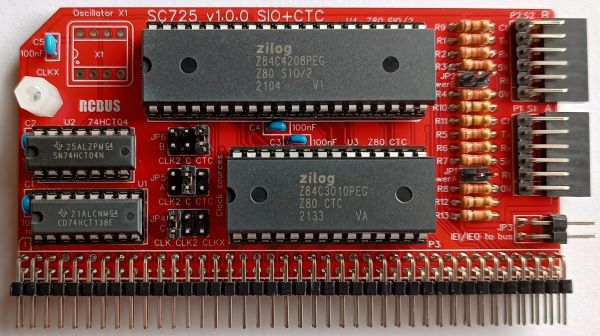
SC725 is a serial and timer module designed for the 80-pin RCBus. It includes a two channel serial interface (Z80 SIO/2) and a 4 channel counter/timer (Z80 CTC). This provides two asynchronous serial ports with optional software controlled baud rates, plus timer functions with interrupts.
- SC725 – Assembly guide
- SC725 – Compatibility
- SC725 – Parts list
- SC725 – Printed circuit board
- SC725 – User guide
- SC700 series information
- SC700 series support
Downloads
- SC725, v1.0, Kit contents sheet (PDF)
- SC725, v1.0, Schematic (PDF)
- SC725, v1.0, PCB design files (OSHWLab)
- SC725, v1.0, Gerber files (ZIP)
Errata
- Nothing known
Suppliers
| Kits | Website | From | Currency |
| Small Computers Direct | SCDirect | UK | GBP |
| Stephen C Cousins | Tindie | UK | USD |
| Small Computer Central | Lectronz | UK | Euro/USD |
| PCBs | Website | From | Currency |
| Small Computers Direct | SCDirect | UK | GBP |
| Stephen C Cousins | Tindie | UK | USD |
| Small Computer Central | Lectronz | UK | Euro/USD |
| Assembled and Tested | Website | From | Currency |
| Not available | |||
| Components | |||
| See parts list |
Tindie does not collect VAT for EU countries
Lectronz does collect EU VAT for orders up to 150 EUR
Parts List
| Reference | Qty | Component |
| PCB | 1 | SC725, v1.0.x, PCB |
| C1 to C5 | 5 | Capacitor, ceramic, 100 nF |
| JP1 and JP2 | 2 | Header, male, 1 row x 2 pin, straight |
| JP3 | 1 | Header, male, 2 row x 2 pin, angled |
| JP4, 5 and 6 | 3 | Header, male, 2 row x 3 pin, straight |
| Jumper | 10 | Jumper shunt |
| P1 and P2 | 2 | Header, male, 1 row x 6 pin, angled |
| P3 | 1 | Header, male, 2 row x 40 pin, angled |
| R1 to R8 | 8 | Resistor, 2k2, 0.25W |
| R9 to R12 | 4 | Resistor, 100k, 0.25W |
| R13 | 1 | Resistor, 10k, 0.25W |
| S1 and S2 | 2 | Header, female, 1 row x 6 pin, angled |
| Screw (for spacer) | 1 | Machine screw, 6mm, M3 |
| Spacer | 1 | Spacer, 10mm, M3, nylon |
| U1 | 1 | 74HCT138 |
| U2 | 1 | 74HCT04 |
| U3 | 1 | Z80 CTC Z84C3008, or Z80 CTC Z84C3010 |
| U4 | 1 | Z80 SIO/2, Z84C4208PEG, or Z80 SIO/2, Z84C4210PEG |
| X1 | 0 | Oscillator, 8-pin Not included in the kit |
| IC socket 16-pin U1 | 1 | Socket, DIP, 16-pin |
| IC socket 14-pin U2 | 1 | Socket, DIP, 14-pin |
| IC socket 28-pin U3 | 1 | Socket, DIP, 28-pin |
| IC socket 40-pin U4 | 1 | Socket, DIP, 40 pin |
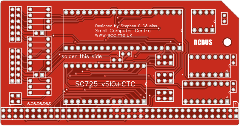
Printed Circuit Board
User Guide
SC725 includes a Z80 SIO/2 which provides two asynchronous serial ports and a Z80 CTC which provides four counter timer channels.
Counter/timer channel 0 can be used to generate a programmable baud rate clock for serial port A. Channel 1 can be used to generate a programmable baud rate clock for serial port B. Alternatively, channels 0 and 1 are free for the user. This choice is made with jumpers 5 and 6.
Counter/timer channels 2 and 3 provide two 8-bit timers which are linked to provide a 16-bit timer. These are typically used to provide periodic interrupts.
Most software and firmware set the SIO divider to 64 and assume the serial clock is 7.3728 MHz. This means the baud rate is the input clock divided by 64. A 7.3728 MHz clock gives 115200 baud.
The baud rate clock is set with jumpers 5 (port A) and 6 (port B). The options are the bus clock (CLK), the second bus clock (CLK2) or one of the CTC outputs. The CTC option is used to provide a software selectable baud rates while the bus clock options provide a fixed baud rates.
The CTC option only works if the software or firmware configures the CTC to generate a suitable clock signal. If in doubt use the CLK or CLK2 options, which bypasses the CTC. If the CPU runs a 7.3728 MHz then CLK will also usually be 7.3728 MHz, so use the CLK option. The CLK2 signal usually requires a clock generator module to be present in the system.
As both the CTC’s timers and the SIO’s internal dividers are used to generate the baud rate, the relationship between them and the firmware and software can cause confusion. The examples below should cover most situations.
In addition, if the CTC’s input clock is not the same signal as the CPU clock, namely the bus clock signal (CLK), there are timing constraints that must be met. This usually means the CTC input clock (CLKC on the schematic) must be the same signal as the bus clock (CLK) or a frequency of less than half that of the bus clock. This must be considered if the optional oscillator (X1) is used. Typically, this will mean that an 18.432 MHz Z180 CPU will require the CTC to be supplied with a 7.3728 MHz clock from CLK2 or X1. With a 7.3728 MHz Z80 CPU the X1 oscillator needs to be less than 3.6864 MHz, so typically a 1.8432 MHz oscillator is used.
The magic numbers
To generate a specific baud rate using a CTC and SIO, the SIO will typically have its divider set to either 16 or 64, while the CTC will be set with a time constant value from 1 to 255. With the CTC having an input clock of 7.3728 MHz, the following CTC time constant values can be used.
| CTC time constant from 7.3728 MHz | Baud rate with SIO divide by 16 |
| 1 | 230400 |
| 2 | 115200 |
| 4 | 57600 |
| 6 | 38400 |
| 12 | 19200 |
| 16 | 14400 |
| 24 | 9600 |
| 48 | 4800 |
| 96 | 2400 |
| 192 | 1200 |
| CTC time constant from 7.3728 MHz | Baud rate with SIO divide by 64 |
| 1 | 57600 |
| 2 | 28800 |
| 3 | 19200 |
| 4 | 14400 |
| 6 | 9600 |
| 12 | 4800 |
| 24 | 2400 |
| 48 | 1200 |
| 96 | 600 |
| 192 | 300 |
To set serial port B’s baud rate to 9600, CTC channel 1’s time constant register must be set to 24 decimal, assuming the SIO is set to divide by 16. This can be achieved by issuing the following two Small Computer Monitor commands:
O 89 55
O 89 18
Or the BASIC commands:
OUT &H89, &H55
OUT &H89, 24
Where:
&H89 is the address of CTC channel 1’s control register (&H88+1)
&H55 selects: No interrupt, Counter mode, Count on rising edge, Time constant follows
24 is the time constant (the divider)
The time constant value 24 selects divide by 48. The doubling of the divider, or halving of the frequency, is caused by the CTC only counting the second edge. Thus baud rate is 7372800 /16/48 = 9600.
Small Computer Monitor, configuration S2, S3, S7, S8
SCM S2/3/7/8 assumes SIO port A is supplied with a 7.3728 MHz clock and sets the SIO port A divider to 64 giving 115200 baud. If the CTC is present it assumes CTC channel 1 has a 7.3728 MHz input clock and configures the CTC to generate a suitable clock for SIO port B to generate the requested baud rate, typically defaulting to 115200 baud.
Note that both the CTC and SIO are configured to generate the required baud rate, so the jumpers must be set as shown or the baud rate may not be sensible.

Warning: Due to limitations in SCM, currently v1.3.1, if a second SIO module is present at address 0x84 and it does not use a CTC, then the baud rate for the serial ports on this module are set for 460800 baud. This is because SCM assumes there is a CTC for this module and configures the SIO as if it has a CTC as a pre-scaler.
Small Computer Monitor, configurations R1, R2, R3, R4
These configurations do not support the CTC but are generally only used on systems with a 7.3728 MHz Z80 CPU. These configurations set both SIO ports to divide 64. with jumpers set as shown below, both ports run at 115200 baud and CTC channels 0 and 1 are not used for baud rate generation.
If the jumpers are set as shown for SCM S2, port A will have a fixed baud rate of 115200 baud while port B will only work if the CTC is set for one of the values in the SIO divide by 64 table above.
RomWBW, platform RCBus, configurations RCZ80_std
The standard configuration of RomWBW, currently v3.5.1, does not have CTC support enabled. The jumpers should be set to bypass the CTC, as illustrated below.
Input/output port functions
| I/O Address | Read | Write |
| 0x80 | SIO Port A control | SIO Port A control |
| 0x81 | SIO Port A data | SIO Port A data |
| 0x82 | SIO Port B control | SIO Port B control |
| 0x83 | SIO Port B data | SIO Port B data |
| 0x88 | CTC 0 counter | CTC 0 control Port A baud rate, or User timer |
| 0x89 | CTC 1 counter | CTC 1 control Port B baud rate, or User timer |
| 0x8A | CTC 2 counter | CTC 2 control Timer low byte |
| 0x8B | CTC 3 counter | CTC 3 control Timer high byte |
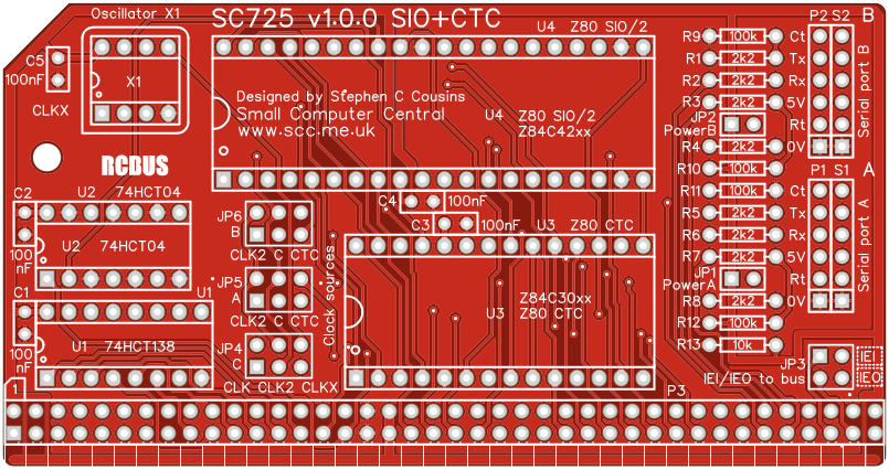
Jumper options
| Jumper | Function |
| JP1 | Power to/from serial port A JP 1.1-2, Connect power to port A The default is jumper shunt not fitted |
| JP2 | Power to/from serial port B JP 2.1-2, Connect power to port B The default is jumper shunt not fitted |
| JP3 | Connects IEI and IEO to bus pins JP 3.1-2, Connect IEI to bus pin 38 JP 3.3-4, Connect IEIOto bus pin 39 The default is jumper shunts not fitted |
| JP4 | Selects CTC channel’s 0,1 and 2 clock input (C) JP 4.1-2, Bus clock signal (CLK) typically 7.3728 MHz JP 4.3-4, Bus clock signal (CLK2) typically 7.3728 MHz JP 4.5-6, Onboard oscillator (X1) typically 7.3728 MHz The default position is a shunt on pins 1-2 |
| JP5 | Selects SIO port A baud rate clock (clock A) JP 4.1-2, Bus clock signal (CLK2) typically 7.3728 MHz JP 4.3-4, Clock source from JP4 (clock C) JP 4.5-6, CTC channel 0 output The default position is a shunt on pins 3-4 |
| JP6 | Selects SIO port B baud rate clock (clock B) JP 4.1-2, Bus clock signal (CLK2) typically 7.3728 MHz JP 4.3-4, Clock source from JP4 (clock C) JP 4.5-6, CTC channel 1 output The default position is a shunt on pins 3-4 |
Connector pin-outs
| P1 and S1 P2 and S2 | Function (serial port) |
| 1 | 0 volt (GND) |
| 2 | RTS (Request to send output) |
| 3 | 5 volts (optional via jumper) |
| 4 | RXD (Receive data input) |
| 5 | TXD (Transmit data output) |
| 6 | CTS (Clear to send input) |
| JP3 | Function (interrupt daisy-chain) |
| 1 | Interrupt enable input (IEI) |
| 2 | Interrupt enable output (IEO) |
Assembly Guide
Below is the suggested order of assembly. A general guide to assembling circuit boards can be found here.

- Resistor R1 to R13
These can be fitted either way around - Sockets for S1 and S2 (angled 6-pin sockets)
Ensure these are fitted flat against the circuit board - Decoupling capacitors C1 to C5 (100 nF)
These can be fitted either way around - Sockets for U1, U2, U3 and U4
- Fit such that the notch in the socket matches the curve in the outline on the PCB silkscreen
- Header pins P1 and P2 (angled 6-pins)
Ensure the pins are parallel to socket S1 and S2 - Bus header P3 (RCBus header pins)
Make sure the pins are parallel to the PCB so that the board is vertical when it is fitted into a backplane socket - Header pins JP3 (angled)
- Header pins for jumpers JP1 and JP2
- Header pins for jumpers JP4, JP5 and JP6
- Insert the integrated circuits into their sockets
Make sure the notch in the component is at the end indicated by the notch in the socket and the curve on the PCB silkscreen - Fit the nylon spacer in the mounting hole
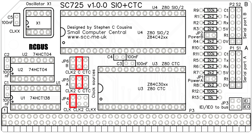
Fit jumper shunts in the positions shown below in red. JP4 selects the clock source to the CTC as the main bus clock (CLK) which is assumed to be 7.3728 MHz. JP5 and JP6 selects this clock as the baud rate clock for both serial ports. At 7.3728 MHz with typical software and firmware the baud rates of both serial ports will be 115200 baud. In this configuration the CTC does not control the baud rates.

Compatibility
This module conforms to the RCBus specification v1.0 for RCBus-2014 and RCBus-Z80.
The RCBus specification includes RCBus-2014 (both RC2014 standard 40-pin bus and RC2014 enhanced 60-pin bus) and also the full 80-pin RCBus. The 80-pin RCBus provides support for advanced Z80 features, such as the interrupt daisy-chain, as well as support for other processor families.
The table below indicates electrical compatibility with each backplane type (40, 60 and 80 pin)

| Backplane | ? | Compatibility notes |
| RCBus 80-pin |  | Fully supported |
| RCBus 60-pin (RC2014 enhanced) | | Limitations: Optional mode 2 interrupt chain requires wires between modules |
| RCBus 40-pin (RC2014 standard) | | Limitations: Optional mode 2 interrupt chain requires wires between modules Some optional signals are not available (CLK2, TX2, RX2) |
Notes
- This product is designed for hobby use and is not suitable for industrial, commercial, or safety-critical applications.
- The product contains small parts and is not suitable for young children.
- RomWBW is copyright Wayne Warthen and has been provided free of charge with his permission.
