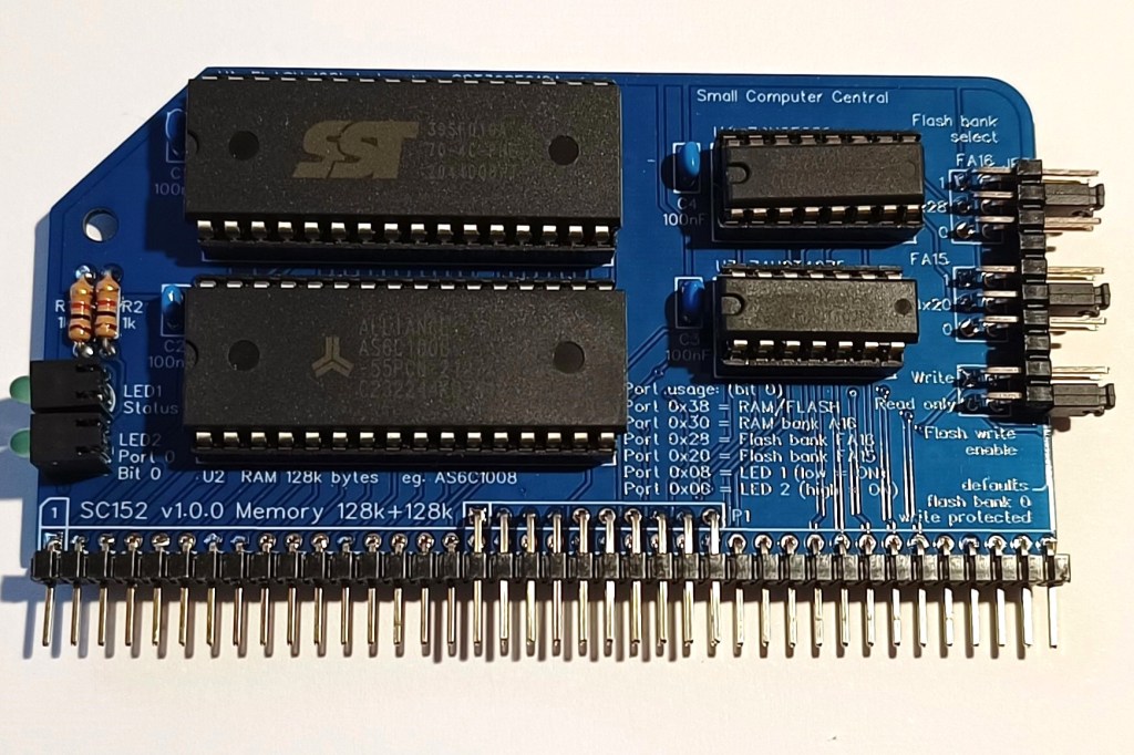
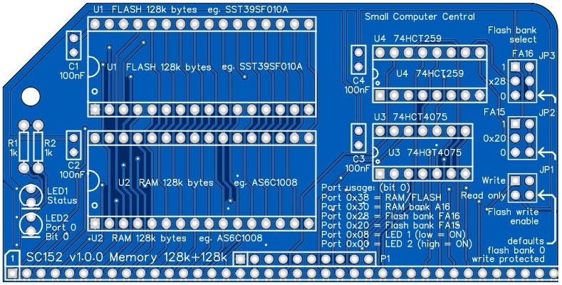
SC152 is a memory module with 128k bytes of FLASH ROM and 128k pages of RAM designed for the RC2014 bus. This module provides suitable memory for running CP/M. It is fully functional on a standard backplane (40 pin), an enhanced backplane (60 pin) and an extended backplane (80 pin).
A later design is now available: SC707
- SC152 – Assembly Guide
- SC152 – Firmware (SCM S8)
- SC152 – Parts List
- SC152 – Printed Circuit Board
- SC152 – Support
- SC152 – User Guide
Downloads
- SC152, v1.0, Kit contents sheet (PDF)
- SC152, v1.0, Schematic (PDF)
- SC152, v1.0, PCB design files (OSHWLab)
- SC152, v1.0, Gerber files (ZIP)
Suppliers
| Kits | Website | From | Currency |
| Small Computers Direct | SCDirect | UK | GBP |
| Stephen C Cousins | Tindie | UK | USD |
| Small Computer Central | Lectronz | UK | Euro/USD |
| PCBs | Website | From | Currency |
| Small Computers Direct | SCDirect | UK | GBP |
| Stephen C Cousins | Tindie | UK | USD |
| Small Computer Central | Lectronz | UK | Euro/USD |
| Assembled and Tested | Website | From | Currency |
| Not available | |||
| Components | |||
| See parts list |
Tindie does not collect VAT for EU countries
Lectronz does collect EU VAT for orders up to 150 EUR
Parts List
| Reference | Qty | Component |
| PCB | 1 | SC152, v1.0, PCB |
| C1 to C4 | 4 | Capacitor, ceramic, 100 nF |
| JP1+2+3 | 1 | Header, male, 2 row x 10 pin, angled |
| Jumper | 3 | Jumper shunt |
| LED1 and 2 | 2 | LED, green, 3mm, angled |
| P1 | 1 | Header, male, 2 row x 40 pin, angled (some pins need to be removed), or header, male, 1 row x 40 pin, angled |
| R1 and R2 | 2 | Resistor, 1k, 0.25W |
| U1 | 1 | FLASH 128k bytes SST39SF010A |
| U2 | 1 | RAM 128k bytes AS6C1008 |
| U3 | 1 | 74HCT4075 |
| U4 | 1 | 74HCT259 |
| IC socket 32-pin U1 and U2 | 2 | Socket, DIP, 32-pin |
| IC socket 14-pin U3 | 1 | Socket, DIP, 14-pin |
| IC socket 16-pin U4 | 1 | Socket, DIP, 16-pin |
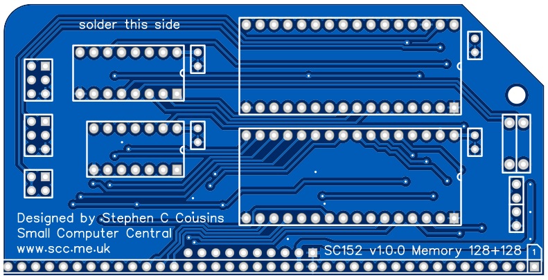
Printed Circuit Board
User Guide
SC152 provides 128k of banked FLASH ROM and 128k bytes of RAM, together with paging control of the lower 32k. This configuration is suitable to run CP/M 2.
At reset the output bits of integrated circuit U4 are all cleared to zero (low voltage). The ROM is paged into memory from 0x0000 to 0x7FFF (32k bytes) with RAM from 0x8000 to 0xFFFF (32k bytes). When input/output address 0x38 bit 0 is set to one (a high voltage) the ROM is paged out and RAM is paged in, giving a full 64k bytes of RAM from 0x0000 to 0xFFFF.
The 128k bytes of FLASH ROM is split into four 32k byte banks. The bank is selected with JP2 (FLASH address A15) and JP3 (FLASH address A16). By default these jumpers should be set to ‘0’ selecting the lowest 32k bytes. By setting jumpers to either 0 or 1, any of the four banks can be selected. Alternatively, these jumpers can be set for software selection of the bank, using output addresses 0x20 bit 0 and 0x28 bit 0.
The 128k bytes of RAM is split into two 64k byte banks. The bank can be selected with output addresses 0x30 bit 0
The status LED should be ON when the system is in reset. With the recommended firmware, the LED should flash OFF for about half a second when the system is released from reset. It should then turn ON and stay on. User software can then control the LED, as required.
Input/output port functions
| I/O Address | Read | Write |
| 0x00 (0x00 to 0x03) | n/a | User LED (LED 2) Low = OFF, high = ON |
| 0x08 (0x08 to 0x0B) | n/a | Status LED (LED 1) Low = ON, high = OFF |
| 0x20 (0x20 to 0x23) | n/a | ROM bank select FA15 |
| 0x28 (0x28 to 0x2B) | n/a | ROM bank select FA16 |
| 0x30 (0x30 to 0x33) | n/a | RAM bank select RA16 |
| 0x38 (0x38 to 0x3B) | n/a | Memory paging (lower 32k) Low = ROM, high = RAM |
Jumper options
| Jumper | Function |
| JP1 | FLASH write enable / protect Read only = Write protected Write = Read and write enabled |
| JP2 | FLASH bank select JP2.1 = FLASH A15 high JP2.2 = Software select FLASH A15 via port 0x20 JP2.3 = FLASH A15 low |
| JP3 | FLASH bank select JP3.1 = FLASH A16 high JP3.2 = Software select FLASH A16 via port 0x28 JP3.3 = FLASH A16 low |
It is recommended that a jumper shunt be fitted in the “Read only” position of JP1 during normal use. It only needs to be in the “Write” position when the contents of the FLASH is to be updated. While the FLASH device requires a very specific sequence of events to protect it against accidental modification, it is best to play safe and use the jumper to ensure it can not be written to.
Assembly Guide
Below is the suggested order of assembly. A general guide to assembling circuit boards can be found here.
- Resistors R1 and R2
These can be fitted either way around - Sockets for U1, U2 and U3
Fit such that the notch in the socket matches the curve in the outline on the PCB silkscreen - Bus header P1
Some pins need to be pulled out of the second row to match the holes in the PCB. Make sure the pins are parallel to the PCB so that the board is vertical when it is fitted into a backplane socket - Decoupling capacitors C1, C2, C3 and C4
These can be fitted either way around - Light emitting diodes LED1 and LED2
Fit such that the short lead and/or small flat on the plastic is at the end marked with a line on the PCB silkscreen - Header pins JP1, JP2 and JP3
This can be one header with a few pins pulled out or three separate headers. Fit a jumper shunts in the “Read only” position of JP1 and in position “0” of JP2 and JP3 - Insert the integrated circuits into their sockets
Make sure the notch in the component is at the end indicated by the notch in the socket and the curve on the PCB silkscreen
Notes
- This design is made in accordance with the “designed for RC2014” labelling scheme.
- RC2014 is a trademark of RFC2795 Ltd.
- This product is designed for hobby use and is not suitable for industrial, commercial, or safety-critical applications.
- The product contains small parts and is not suitable for young children.
