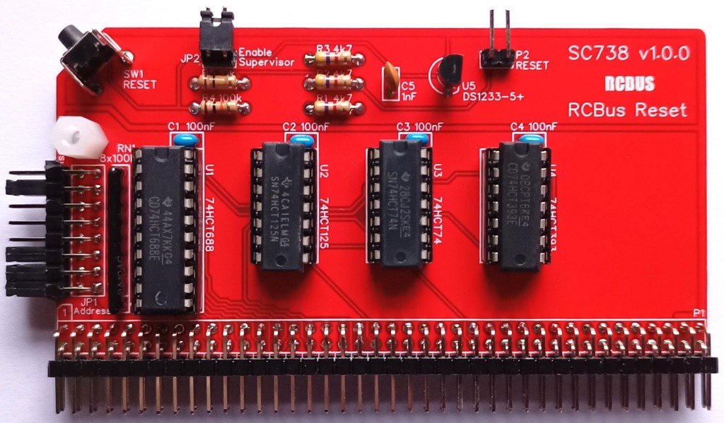
SC738 is a reset module designed for the RCBus. It provides a clean power on reset, a debounced reset button, and a means to force a hardware reset with a simple port write.
- SC738 – Assembly guide
- SC738 – Compatibility
- SC738 – Parts list
- SC738 – Printed circuit board
- SC738 – User guide
- SC700 series information
- SC700 series support
Downloads
- SC738, v1.0, Kit contents sheet (PDF)
- SC738, v1.0, Schematic (PDF)
- SC738, v1.0, PCB design files (OSHWLab)
- SC738, v1.0, Gerber files (ZIP)
Errata
- Nothing known
Suppliers
| Kits | Website | From | Currency |
| Small Computers Direct | SCDirect | UK | GBP |
| PCBs | Website | From | Currency |
| Small Computers Direct | SCDirect | UK | GBP |
| Assembled and Tested | Website | From | Currency |
| Not available | |||
| Components | |||
| See parts list |
Tindie does not collect VAT for EU countries
Lectronz does collect EU VAT for orders up to 150 EUR
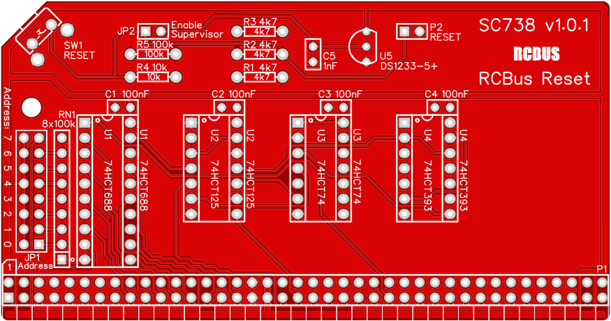
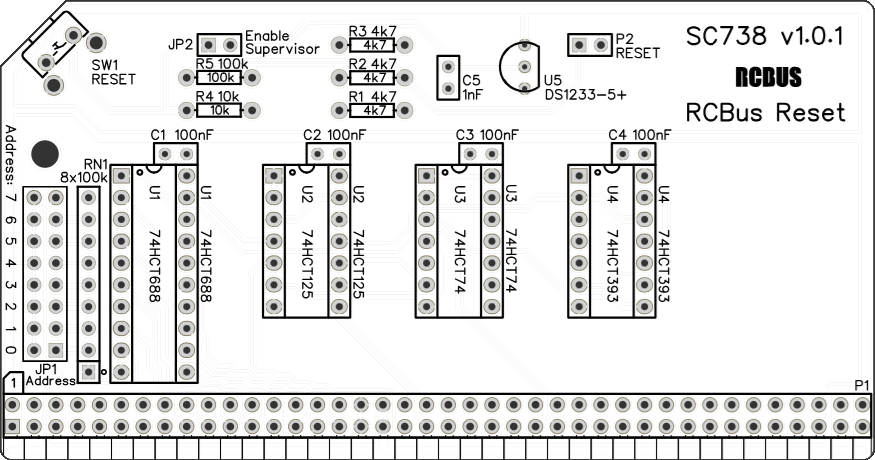
Parts List
| Reference | Qty | Component |
| PCB | 1 | SC738, v1.0, PCB |
| C1 to C4 | 4 | Capacitor, ceramic, 100 nF |
| C5 | 1 | Capacitor, ceramic, 1 nF |
| JP1 | 1 | Header, male, 2 row x 8 pin, angled |
| JP2 | 1 | Header, male, 1 row x 2 pin, angled |
| Jumper | 9 | Jumper shunt |
| P1 | 1 | Header, male, 2 row x 40 pin, angled |
| P2 | 1 | Header, male, 1 row x 2 pin, angled |
| R1 to R3 | 3 | Resistor, 4k7, 0.25W |
| R4 | 1 | Resistor, 10k, 0.25W |
| R5 | 1 | Resistor, 100k, 0.25W |
| RN1 | 1 | Resistor network, 8x100k, SIL, 9-pin |
| SW1 | 1 | Switch, tactile button, angled |
| Screw (for spacer) | 1 | Machine screw, 6mm, M3 |
| Spacer | 1 | Spacer, 10mm, M3, nylon |
| U1 | 1 | 74HCT688 |
| U2 | 1 | 74HCT125 |
| U3 | 1 | 74HCT74 |
| U4 | 1 | 74HCT393 |
| U5 | 1 | DS1233-5+ supervisor |
| IC socket 20-pin U1 | 1 | Socket, DIP, 20-pin |
| IC socket 14-pin U2 to U4 | 3 | Socket, DIP, 14-pin |
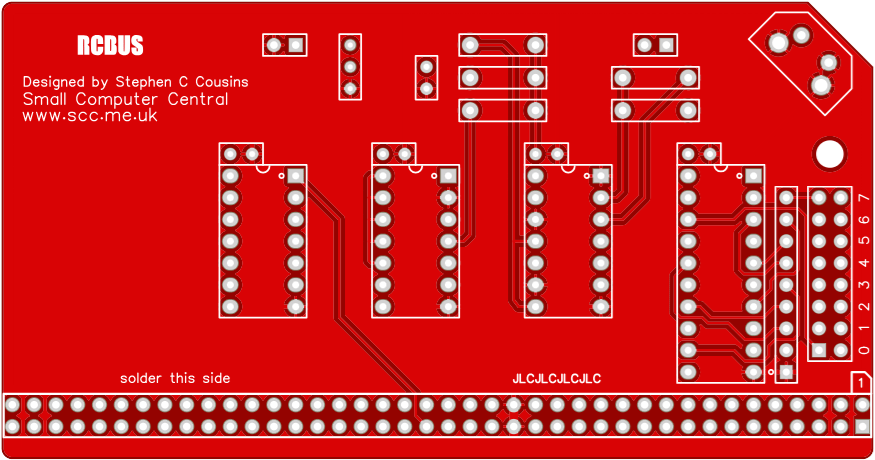
Printed Circuit Board
User Guide
SC738 is a module dedicated to generating a system reset signal.
The system reset signal is generated at power up, upon pressing switch SW1, or with an external switch connected to P2. The power up reset is generated by the voltage supervisor U5. The supervisor will also hold the system in reset if the 5-volt supply drops below about 4.75 volts. In addition, the supervisor cleans up the reset signal generated with the reset button.
A hardware reset can also be generated by writing to the I/O port address selected with JP1. The suggested address is 47 hexadecimal (71 decimal). The value written to the port is irrelevant, any value will work. A clean reset signal is generated that lasts 128 clock cycles, typically approximately 17 microseconds.
To initiate a hardware reset from an assembler program:
OUT ($47), A
To initiate a hardware reset from SCM, enter the command:
O 47 0
To initiate a hardware reset from BASIC, enter the command:
OUT 71, 0
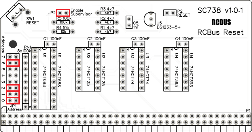
The system should only have one enabled voltage supervisor. If there is another one in the system, one of them needs to be disabled. The circuit on this module is likely to be the best one, so ideally keep this one enabled and disable any others. To enable the supervisor on this module, fit a jumper shunt to header pins JP2.
Input/output port functions
| RCBus I/O Address | Read | Write |
| Configurable *1 | n/a | Trigger reset on write |
- The RCBus I/O base address should be set to match the software you are using. Typically, this is 0x47 (jumper shunts fitted for bits 0 , 1, 2, 6).
Jumper options
| Jumper | Function |
| JP1 | Set module’s RCBus I/O address The default is 0x47 |
| JP2 | Enable voltage supervisor |
Connectors
| Connector | Function |
| P 1 | RCBus connector |
| P 2 | Header pins, optional external reset switch |
Assembly Guide
Below is the suggested order of assembly. A general guide to assembling circuit boards can be found here.
- Resistors R1, 2, 3 (4k7), R4 (10k), R5 (100k)
These can be fitted either way around - Decoupling capacitors C1 to C4 (100 nF)
These can be fitted either way around - Capacitor C5 (1 nF)
These can be fitted either way around - Sockets for U1 to U4
Fit such that the notch in the socket matches the curve in the outline on the PCB silkscreen - Resistor network RN1 (8 x 100k)
These must be fitted the correct way around whereby the dot on the component matches the dot on the PCB silkscreen - Header pins P2 (1 row x 2 pin, angled)
- Header pins JP2 (1 row x 2 pin, angled)
- Bus header P1
Make sure the pins are parallel to the PCB so that the board is vertical when it is fitted into a backplane socket - Header pins JP1 (2 row x 8 pin, angled)
- Switch SW1
- Voltage supervisor U5
Carefully bend the legs to match the hole spacing on the PCB and ensure the orientation matches the markings on the PCB - Insert the integrated circuits into their sockets
Make sure the notch in the component is at the end indicated by the notch in the socket and the curve on the PCB silkscreen - Fit the nylon spacer in the mounting hole
Fit jumper shunts in the positions shown below. All other jumpers are optional and should only be fitted if the feature is required.
Compatibility
This module conforms to the RCBus specification v1.0 for RCBus-2014 and RCBus-Z80.
The RCBus specification includes RCBus-2014 (both RC2014 standard 40-pin bus and RC2014 enhanced 60-pin bus) and also the full 80-pin RCBus. The 80-pin RCBus provides support for advanced Z80 features, such as the interrupt daisy-chain, as well as support for other processor families.
The table below indicates electrical compatibility with each backplane type (40, 60 and 80 pin)

| Backplane | ? | Compatibility notes |
| RCBus 80-pin |  | Fully supported |
| RCBus 60-pin (RC2014 enhanced) | | Fully supported |
| RCBus 40-pin (RC2014 standard) | | Fully supported |
Notes
- This product is designed for hobby use and is not suitable for industrial, commercial, or safety-critical applications.
- The product contains small parts and is not suitable for young children.
