SC724 is a prototyping breakout module designed for the RCBus.
- SC724 – Assembly guide
- SC724 – Compatibility
- SC724 – Parts list
- SC724 – Printed circuit board
- SC724 – User guide
- SC700 series information
- SC700 series support
Downloads
- SC724, v1.0, Kit contents sheet (PDF)
- SC724, v1.0, Schematic (PDF)
- SC724, v1.0, PCB design files (OSHWLab)
- SC724, v1.0, Gerber files (ZIP)
Errata
Nothing known
Suppliers
| Kits | Website | From | Currency |
| Small Computers Direct | SCDirect | UK | GBP |
| Stephen C Cousins | Tindie | UK | USD |
| Small Computer Central | Lectronz | UK | Euro/USD |
| PCBs | Website | From | Currency |
| Small Computers Direct | SCDirect | UK | GBP |
| Stephen C Cousins | Tindie | UK | USD |
| Small Computer Central | Lectronz | UK | Euro/USD |
| Assembled and Tested | Website | From | Currency |
| Not available | |||
| Components | |||
| See parts list |
Tindie does not collect VAT for EU countries
Lectronz does collect EU VAT for orders up to 150 EUR
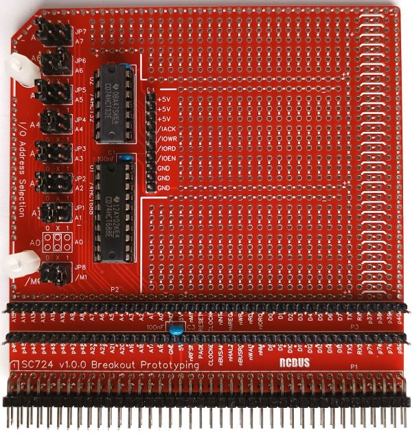
Parts List
| Reference | Qty | Component |
| PCB | 1 | SC724, v1.0, PCB |
| C1 to C3 | 3 | Capacitor, ceramic, 100 nF |
| JP1 to JP8 | 8 | Header, male, 2 row x 3 pin, straight |
| Jumper | 8 | Jumper shunt |
| P1 | 1 | Header, male, 2 row x 40 pin, angled |
| P2 and P3 | 2 | Header, male, 1 row x 40 pin, straight |
| P4 | 1 | Header, male, 1 row x 10 pin, straight |
| U1 | 1 | 74HCT688 |
| U2 | 1 | 74HCT32 |
| Spacer | 2 | Spacer, 10mm, M3, nylon |
| Screw (for spacer) | 2 | Machine screw, 6mm, M3 |
| IC socket 20-pin U1 | 1 | Socket, DIP, 20-pin |
| IC socket 14-pin U2 | 1 | Socket, DIP, 14-pin |
Printed Circuit Board
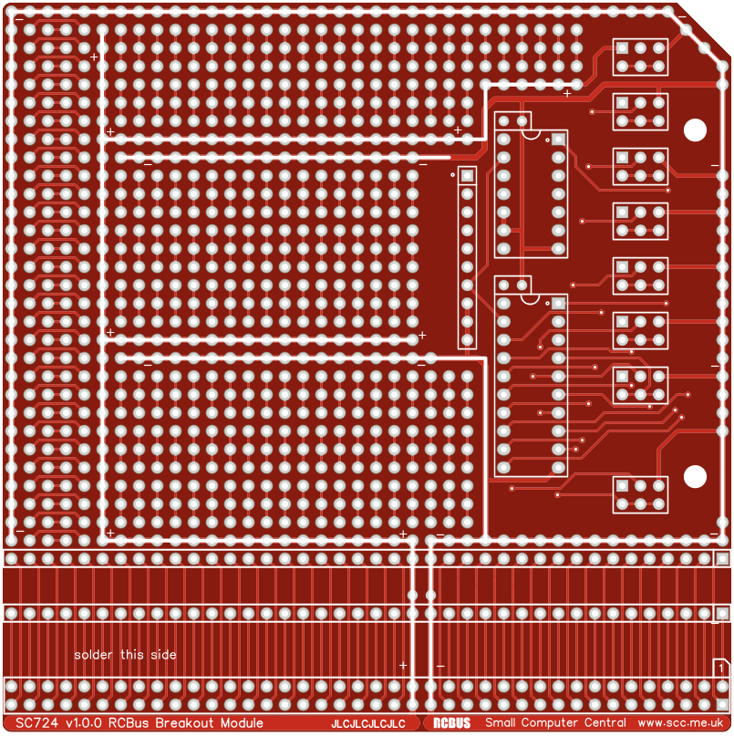
PCB dimensions: RCBus 80-pin “large” size module 4.0″ x 4.0″
User Guide
The prototyping breakout module can be used to breakout signals to an external prototype or it can host a complete prototype built on the module.
As a breakout module it provides easy access to all bus signals as well as configurable device enable, device write, device read and interrupt acknowledge signals. Typically these will be accessed with dupont cables connected to P2, P3 and P4.
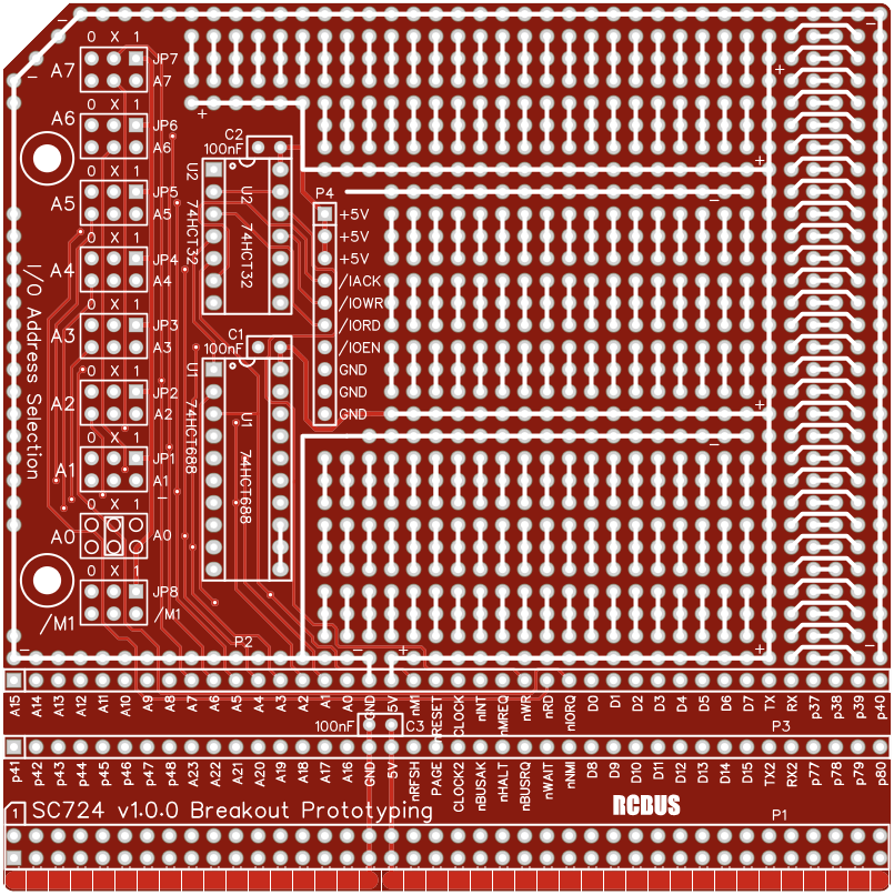
Input/output port functions
| I/O Address | Read | Write |
| Configurable | custom | custom |
Jumper options
| Jumper | Function |
| JP 1 to 7 | Select required states of address lines A1 to A7 JPx.1, address line Ax must be high JPx.2, address line Ax can be high or low (don’t care) JPx.3, address line Ax must be low A0 is hard wired to “don’t care” |
| JP 8 | Select required state of the /M1 signal JP8.1, /M1 signal must be high JP8.2, /M1 signal can be high or low (don’t care) JP8.3, /M1 signal must be low Usually, /M1 is set for “must be high” |
Connector pin-outs
| P1 | Function |
| 1 to 80 | RCBus 80-pin (see RCBus specification) |
| P2 | Function |
| 1 to 40 | RCBus pins 1 to 40 (see RCBus specification) |
| P3 | Function |
| 1 to 40 | RCBus pins 41 to 80 (see RCBus specification) |
| P4 | Function |
| 1 | +5 volts |
| 2 | +5 volts |
| 3 | +5 volts |
| 4 | /INTACK = Interrupt acknowledge /INTACK = /M1 low and /IORQ low |
| 5 | /IOWR = Write to selected output address /IOWR = /IOEN low and /WR low |
| 6 | /IORD = Read from selected input address /IORD = /IOEN low and /RD low |
| 7 | /IOEN = Enable selected Input/output address /IOEN = /IORQ low and /M1 as JP8 and A# as JP# |
| 8 | GND |
| 9 | GND |
| 10 | GND |
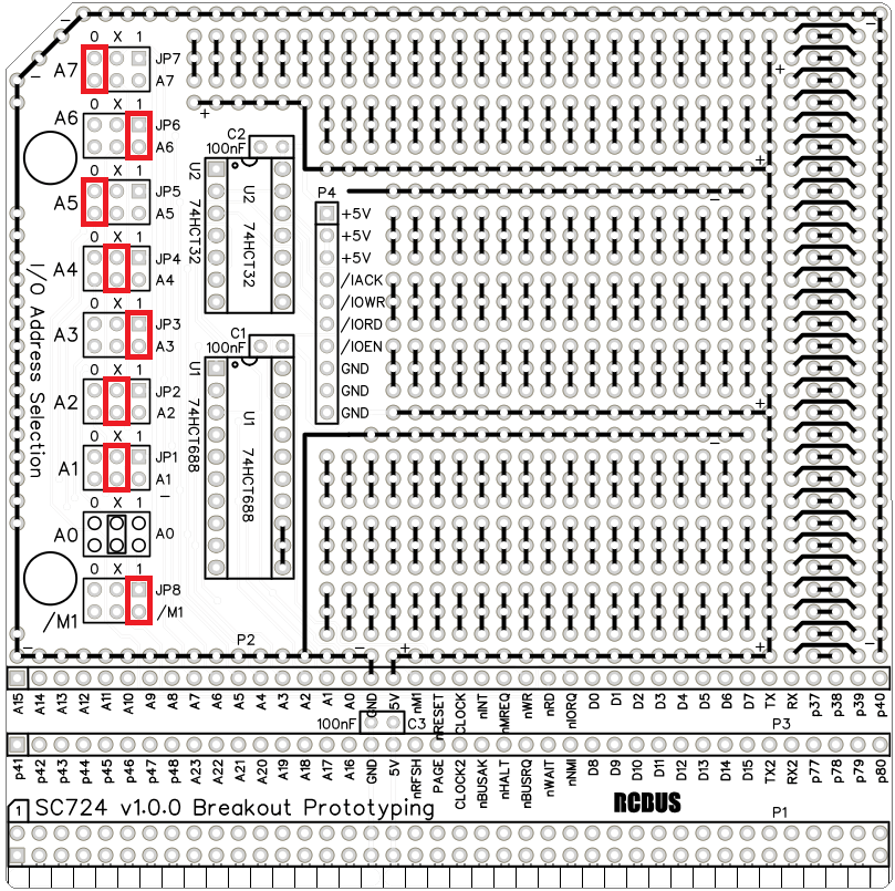
Address selection
The input/output device address is selected with jumpers JP1 to JP8. Each jumper allows the required state of A1 to A7 and /M1 to be set for high, low or don’t care. Don’t care means the signal can be either high or low. A0 does not have a jumper and is always wired as don’t care. The tightest address decoding is thus two input/output addresses.
In the example below, jumper shunts fitted in the highlighted positions select the address of an input/output device as binary 010X 1XXX with /M1 high, where X is don’t care (either high or low). In hexadecimal the address range selected is 48 to 4F, with a ghost address range of 58 to 5F. The ghost address range exists because A4 is don’t care and is typical of modules that don’t have tight address decoding. For example, when a 74HCT138 is used for address decoding. The 74HCT138 only has seven inputs and can not fully decode some address ranges.
Assembly Guide
Below is the suggested order of assembly. A general guide to assembling circuit boards can be found here.

Only fit header pins P2 and P3 if you intend using this module to breakout signals to an external prototype using Dupont wires (or similar). If building a prototype on this module it is best to leave these header pins off and use the holes for wiring.
- Decoupling capacitors C1 to C3
These can be fitted either way around - Bus header pins P1
- Header pins JP1 to JP8
- Header pins P4
- Header pins P2 and P3 (optional)
Compatibility
This backplane conforms fully to the RCBus specification v1.0 and thus supports: RCBus-2014, RCBus-Z80, RCBus-68xx, RCBus-9995.
The RCBus specification includes RCBus-2014 (both RC2014 standard 40-pin bus and RC2014 enhanced 60-pin bus) and also the full 80-pin RCBus. The 80-pin RCBus provides support for advanced Z80 features, such as the interrupt daisy-chain, as well as support for other processor families.
The table below indicates electrical compatibility with each backplane type (40, 60 and 80 pin)

| Backplane | ? | Compatibility notes |
| RCBus 80-pin |  | Fully supported |
| RCBus 60-pin (RC2014 enhanced) | | Limitations: Only 60-pin bus signals available |
| RCBus 40-pin (RC2014 standard) | | Limitations: Only 40-pin bus signals available |
Notes
- This product is designed for hobby use and is not suitable for industrial, commercial, or safety-critical applications.
- The product contains small parts and is not suitable for young children.
