In part 1 of this series we took a very quick tour through the whole process of designing a product. In part 2 and part 3 we designed the electronics for a digital I/O module. We will now design the circuit board.
As described in part 1, we will use EasyEDA.com software to draw the schematic and layout the circuit board.
EasyEDA is constantly improving their software so what follows may become dated over time. Also, this is only a very brief tutorial. You will need to experiment to discover the vast majority of the software’s features.
While it is not strictly necessary to draw your schematic in EasyEDA, it is highly recommended that you do. If you just use EasyEDA to layout a circuit board you miss out on many features in the software which show you where connections are missing or where unwanted connections have been made. If you use the schematic feature you shouldn’t make any routing errors on the circuit board.
With the schematic drawn in EasyEDA, the software knows which components are connected to which. The links are either drawn with individual lines (or “wires”) on the schematic or have labels to identify a connection. The software is able to maintain a list of these connections, known as a Net List.
Each component drawn on the schematic must have an associated component footprint. This allows the software to draw that component accurately on the circuit board layout and to know which pads require connections.
The components on the schematic can be found in the schematic library, whilst those on the circuit board are found in the PCB library. Each library has many common components provided for you. If the required component is not there (or you don’t like the look of it) you can look in other libraries, such as people you follow, or in your own work space. You can create your own components if you wish.
Schematic capture
The process of transferring your circuit design to EasyEDA is called Schematic Capture. This is just a posh term for drawing your circuit diagram!
Follow the method in part 1 to create a project and draw the schematic. You should end up with something like this:
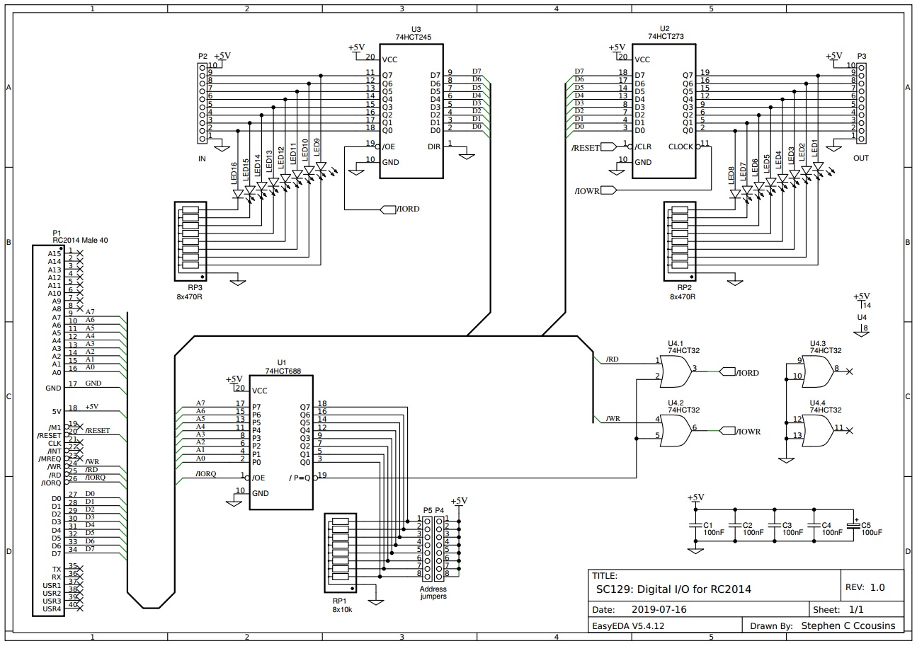
Take your time and make sure your schematic is correct or you will likely copy those errors to your circuit board.
Here are a few things to consider and to watch out for:

The red circle (above) indicates where the vertical line does not end exactly on the horizontal line it is supposed to be joining. If it is drawn correctly a black dot is shown to indicate the connection. Leaving this error on the schematic could result in you not making this connection on the circuit board layout, as the software will not know it is supposed to be there.
The yellow circle also indicates an inaccurately drawn line. If drawn accurately it will just touch the component and not be highlighted with a black dot. In this case the connection is still valid and is only a cosmetic issue.
The orange circle indicated where a “netLabel” is not touching the line and will not be associated with that line. This error could also result in you not making a connection on the circuit board. The green circle indicates a correctly placed label. When you drag the label across the schematic the software indicates the connection point to guide you.
The blue circle indicates an alternative label style. Both styles create an entry in the net list, so you can use either.
Circuit board layout
From EasyEDA designer’s menu, select “Convert to PCB”. This will create a printed circuit board file.

One of the really powerful features of this software is the ability to go back and make changes to the schematic, then select “Update PCB” to have only the changes copied over to the PCB layout.
Initially the PCB layout will look something like this:
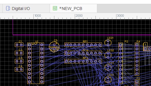
The pink line is the circuit board outline. The components are shown underneath. The blue lines, called Ratlines, show all the connections required to match the schematic’s net list.
As we are designing a module for the RC2014 bus we need to change the PCB outline to a more suitable one. First select the pink outline and delete it. Now select Libraries and search for RC40 in the PCB Modules section, as shown below. In this example I’m using the less common 40 pin module size. Most RC2014 modules use a 39 pin connector. Either are suitable for this project.

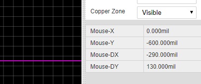
Select “RC40 Module Outline” (owner sccousins) and place it on the PCB layout. Position it carefully so the origin is at coordinates 0,0 which helps when positioning other components later on. This can be done by watching the Mouse-X and Mouse-Y values and moving until X=0.000mil and Y=-600.000mil. This odd Y value is simply due to the reference point on the outline not being at the top left corner of this particular PCB outline.
Drag the components into the desired position within the board outline. Where possible, components should be placed to reduce the mess of ratlines. This is achieved by putting associated components close together and by rotating for flipping components. You should end up with something like this:

Using the RC40 outline the first hole in the bus connector should be at coordinates 50.000, 1850.000 mil.
EasyEDA has an Auto-route feature which will route tracks to all the required locations. This is selected from the menu and any preferences set in the resulting dialog box. I prefer to use wider tracks than the defaults in EasyEDA so I would select something like 10 mil rather than the default 6 mil. When the routing is complete you should see something like this:

I prefer to manually route my boards. I like to run good power supply lines and ensure short paths to the decoupling capacitors. I also like to reduce the number of tracks that run between component pins on the solder side (but that is probably not really important – just one of my hang-ups). To be fair, you can fine tune the auto-router to improve the results, but where’s the fun in that?
Once the tracks are in position the silkscreen legends on the top and bottom of the boards can be fine tuned. A board with a complete set of component references and values is much easier to work on than one with less detail. Additional text and graphics can be added where appropriate.
The final stages are really optional but recommended. A copper pour can be used to ‘fill’ unused space on the board. This helps with EMI screening and reduces ground impedance. Another feature worth using is to add tear drops to the junction of pads and tracks. These junctions can be a weak spots so teardrops can be added to provide a kind of strain relief.
Really important stuff
Always, always, use the design manager to check all connections in the net list have been made and there are no DRC errors. If you have missed a connection that should have been made, the “Nets” list will show it. Also the board will have a ratline still showing (but these are easy to miss). The Design Rule Checker (DRC) will tell you if any connections have been made that shouldn’t have been and if any design rules have been violated. You need to refresh these lists by clicking the refresh icon next to each of them.
Never, ever, order boards without using the design manager to check for Net errors and DRC errors. NEVER.
The end result
EasyEDA has a feature, called Photo View, to produce a render image of the board. Here is the rendered image of the board I designed.

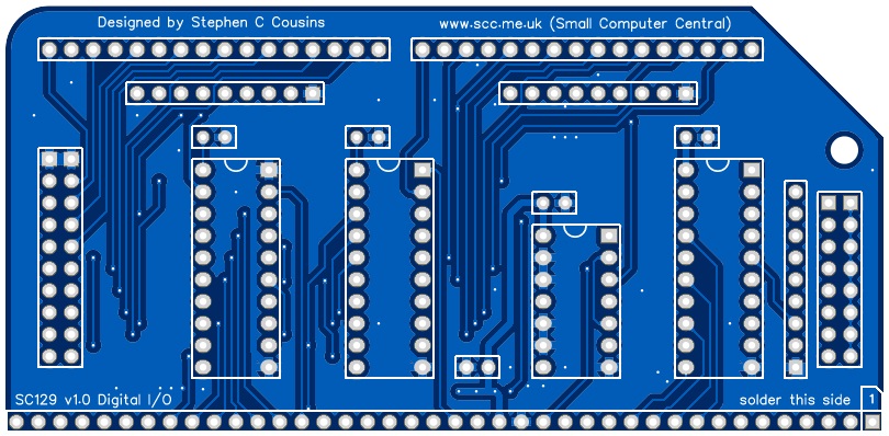
I got some green boards made and this is the end result:
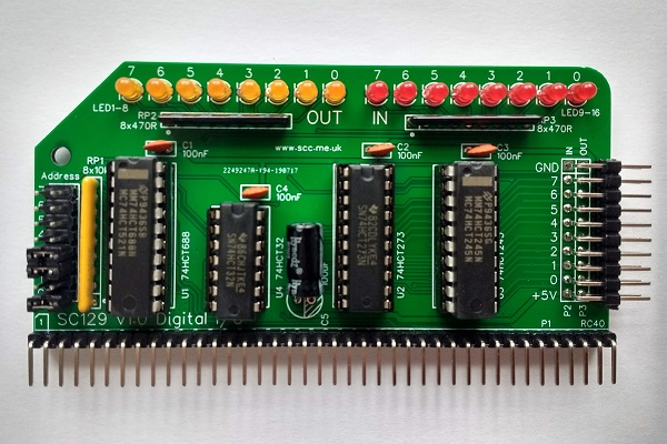
I actually made a mistake on the silkscreen of this board. I have the input and output bit numbers upside down. Drat. Bit zero should be at the top. The tracks are all correct, thanks to the net list feature as good as telling me where to put them, but when it came to drawing some simple numbers I didn’t check. Otherwise, the board works great.
I’ll be the first to admit this series is only a brief guide to design and there is a lot of detail missing, so there will be lots of trial and error learning. However, I have found it well worth persevering and really getting to grips with EasyEDA. Getting boards made in China is surprisingly cheap and the results are amazingly good. Hand made bird’s nest prototypes have nothing on a professional looking PCB. I therefore encourage you to give it a try. If you get as far as receiving your first working PCB in the post, I very much doubt you will regret the effort.
