In part 2 of this series we started designing the electronics for our digital I/O interface. In this part we will complete the schematic.
Output Port
Our specification calls for an 8-bit digital output port with an LED indicator for each output.
The easiest way to add an LED to indicate the state of an output is illustrated below.
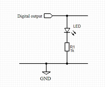
The value of the current limiting resistor (R1) can be anywhere between about 330 ohms and 1000 ohms depending on the sensitivity of the LED and the desired brightness. For general use I tend to use 470R or 1k.
In part 2 of this series, we designed the address decoding to provide a signal (/IOWR) which is active when the processor is wanting to write to the 8 digital outputs. When this signal is active (low) the digital I/O module must latch the state of the 8 data bus signals to the output port. The new state of the outputs must then be remembered by the output port until the processor changes them.
The usual way to implement this is to use an 8-bit register (or latch). When the /IOWR signal is inactive (high) the register remains unchanged. When the /IOWR signal is active (low) the data can be transferred to the register. Ideally, the data should be latched into the register on the rising edge of the /IOWR signal as this gives the maximum time for everything to settle.
There are several 74 series chips which could be used for this. We will use a 74HCT273. This chip has the advantage of a CLEAR input. By connecting this input to the processor’s RESET signal, the port is cleared (all outputs off) when the processor resets.
This gives us the following digital output port circuit.
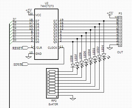
P3 is the connector where the output signals are available for external connection.
LED1 to LED 8 indicate the state of each of the 8 digital outputs. The LED will be ON when the output is set high.
RP2 is a resistor network (or resistor pack). We could use 8 separate resistors but in this case we are using a package containing 8 resistors. These take up less room on the circuit board and are quicker to assemble. They don’t look as pretty or as retro though.
U2 is the 74HCT273. Pin 1 is the CLEAR input. When this input is low the register is cleared and thus all outputs are turned OFF. This is used to turn the outputs off when processor is RESET. Pin 11 is the latch signal. As this signal transitions from low to high the data on the data bus is latched into the register and the outputs are driven high or low accordingly. The outputs remain in this state until the next /IOWR or /RESET.
The signals /IOWR and /RESET are not drawn with a line going right back to their source but are instead shown with “label” shapes (or “Net Port” as EasyEDA calls them). This is sometimes used to avoid having lots of lines crossing each other which can be hard to follow. It also has another convenient use here; this part of the schematic can be shown in isolation as self-explanatory labels are shown rather than lines just disappearing off the edge of the schematic.
The data bus is drawn on the left as a signal thick line (a “Bus”) rather than cluttering up the schematic with 8 lines all going to the same places. All signals joining and leaving the bus should be labelled, as shown above for D0 to D7. The label needs to be attached to the signal line; it is not just a piece of text near the line. EasyEDA calls these a “Net Label”. Proper labelling is important as the schematic is not just a simple picture; it is linked to the circuit board design where all signals must be part of a “Net List”. The benefits of this are enormous as we will see when designing the circuit board.
Input Port
Our specification calls for an 8-bit digital input port with an LED indicator for each input.
As with the output port, the easiest way to add an LED to indicate the state of an input is to just connect an LED and current limit resistor to each input.
The only disadvantage of this simple LED circuit is that it presents a significant load to the source of the signal we are wanting to read (or “input”). There may be some cases where this is undesirable. The solution would be to add a buffer between the input signal and the LED. In this case we want a nice simple design so we will not include a buffer.
The address decoding circuit provides a signal (/IORD) which is active when the processor is wanting to read the state of the 8 digital inputs. When this signal is active (low) the digital I/O module must place the state of the digital inputs on the data bus.
The usual way to implement this is to use an 8-bit buffer which has tri-state outputs. When the /IORD signal is inactive (high) the buffer’s outputs are tri-state. Tri-state means the outputs of the buffer are not driving the data bus high or low. This is required as the data bus is shared by all devices in the system and only one of them can be driving the data bus. When the /IORD signal is active (low) the buffer drives the data bus signals high or low depending on the state of the buffer’s inputs. Thus the processor can “see” the state of the 8 inputs on the data bus.
There are several 74 series chips which could be used for this. We will use a 74HCT245. This chip is bi-directional but here we only need it to work in one direction. This seems an overkill but it is desirable to only stock a limited range of chips.
This gives us the following digital input port circuit.

P2 is the connector where the input signals are connected to our digital I/O module.
LED9 to LED 16 indicate the state of each of the 8 digital inputs.
RP3 is a resistor network (or resistor pack) providing current limiting for the LEDs.
U3 is the 74HCT245. Pin 19 is the output enable input. When high the outputs are tri-state. When low the outputs are driven high or low depending on the buffer’s input states. Pin 1 is the direction select input. This chip is bidirectional but we are only using it in one direction, so this input is fixed low.
The Complete Schematic
We have now finished the design of all the blocks on our block diagram so we can combine them for a complete schematic.
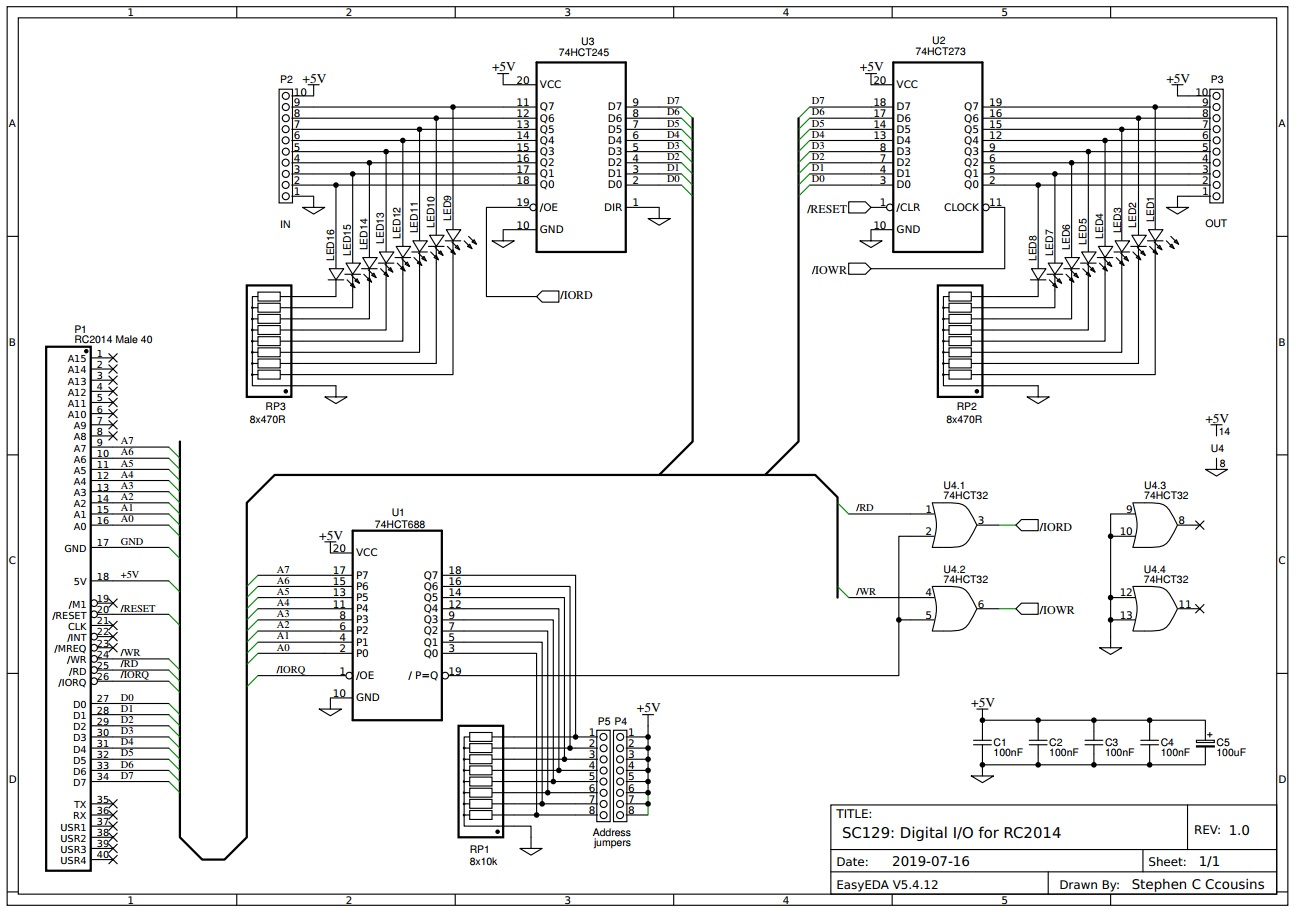
The inputs of the unused OR gates are tied to ground as inputs should not be left floating. Unused signals on the schematic are terminated with a cross to clarify that they will not be found elsewhere on the diagram.
The capacitors, C1 to C4, are called decoupling or bypass capacitors. These are required to reduce noise generated by the digital chips as they rapidly switch state. It is usual to find one of these fitted close to each integrated circuit on a printed circuit board, however, they are often shown on a schematic in a group for convenience.
It is also common to see a larger capacitor, like C5, which is included to help suppress lower frequency transients on the supply lines. This is particularly desirable on a circuit that can switch higher current loads, which could be the case here depending on what the output port is connected to.
As this design is being built as an RC2014 module the schematic includes an RC2014 bus connector. To convert the design to a different modular Z80 system, such as the LiNC Z50Bus, only the bus connector need be changed on the schematic.
In the next instalment we will design the printed circuit board.
