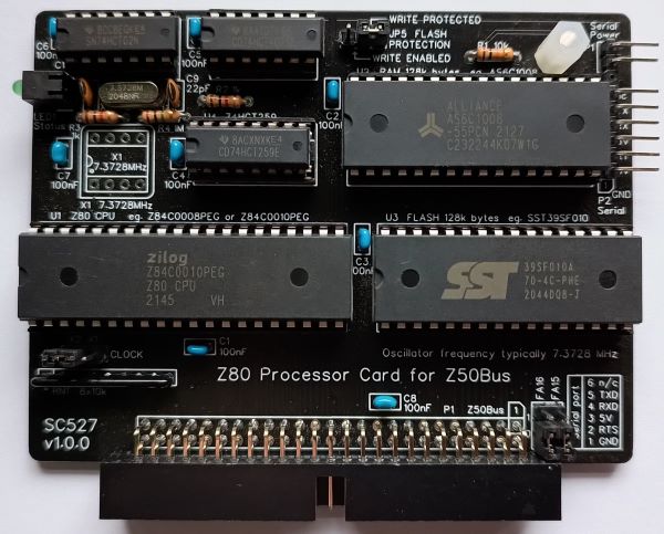
SC527 is a Z80 processor card designed for the Z50Bus. It includes a Z80 CPU, 128k FLASH ROM, 128k RAM, clock oscillator and a simple serial port.
- SC527 – Assembly Guide
- SC527 – Firmware (SCM F1)
- SC527 – Parts List
- SC527 – Printed Circuit Board
- SC527 – Support
- SC527 – User Guide
Downloads
- SC527 – Kit contents sheet (PDF)
- SC527 – Schematic v1.0 (PDF)
- SC527, v1.0, PCB design files (OSHWLab)
- SC527, v1.0, Gerber files (ZIP)
Suppliers
| Kit Suppliers | Website | Ships from |
| Stephen C Cousins | Tindie | UK |
| Small Computer Central | Lectronz | Euro/USD |
| PCB Suppliers | Website | Ships from |
| Stephen C Cousins | Tindie | UK |
| Assembled and Tested | Website | Ships from |
| Not available | ||
| Component Suppliers | ||
| See parts list |
Parts List
| Reference | Qty | Component |
| PCB | 1 | SC527, v1.0, PCB |
| C1 to C8 | 8 | Capacitor, ceramic, 100 nF |
| C9 and C10 | 2 | Capacitor, ceramic, 22 pF |
| JP1 | 1 | Header, male, 1 row x 2 pin, angled |
| JP2, 3, 4,5 | 4 | Header, male, 1 row x 3 pin, straight |
| Jumper | 5 | Jumper shunt |
| LED1 | 1 | LED, green, 3mm, angled |
| P1 | 1 | Box header, 2 x 25 pin, angled, or Header, male, 2 row x 25 pin, angled |
| P2 | 1 | Header, male, 1 row x 6 pin, angled |
| R1 | 1 | Resistor, 10k, 0.25W |
| R2 and R3 | 2 | Resistor, 1k, 0.25W |
| R4 | 1 | Resistor, 1M, 0.25W |
| RN1 | 1 | Resistor network, 8x10k, SIL, 9-pin |
| Spacer | 1 | Spacer, 10mm, M3, nylon |
| Screw (for spacer) | 1 | Machine screw, 6mm, M3 |
| U1 | 1 | Z80 CPU, Z84C0008PEG, or Z80 CPU, Z84C0010PEG |
| U2 | 1 | RAM 128k bytes, AS6C1008 |
| U3 | 1 | FLASH 128k bytes, SST39SF010A |
| U4 | 1 | 74HCT259 |
| U5 | 1 | 74HCT4075 |
| U6 | 1 | 74HCT02 |
| X1 | 1 | Oscillator 7.3728 MHz (optional. not included in kit) |
| X2 | 1 | Crystal, 7.3728MHz |
| IC socket 40-pin U1 | 1 | Socket, DIP, 40-pin |
| IC socket 32-pin U2 and U3 | 2 | Socket, DIP, 32-pin |
| IC socket 16-pin U4 | 1 | Socket, DIP, 16-pin |
| IC socket 14-pin U5 and U6 | 2 | Socket, DIP, 14-pin |
Printed Circuit Board


User Guide
SC527 only requires power and a reset signal to be a complete working computer. The recommended firmware is the Small Computer Monitor (SCM). With the addition of a Compact Flash interface and card this card is able to run CP/M 2.
At reset the output bits of integrated circuit U4 are all cleared to zero (low voltage). The FLASH ROM is paged into memory from 0x0000 to 0x7FFF (32k bytes) with RAM from 0x8000 to 0xFFFF (32k bytes). When input/output address 0x38 bit 0 is set to one (a high voltage) the ROM is paged out and RAM is paged in, giving a full 64k bytes of RAM from 0x0000 to 0xFFFF.
The 128k bytes of FLASH ROM is split into four 32k byte banks. The bank is selected with JP3 (FLASH address A15) and JP4 (FLASH address A16). By default these jumpers should be set to ‘0’ selecting the lowest 32k bytes. By setting jumpers to either 0 or 1, any of the four banks can be selected.
The 128k bytes of RAM is split into two 64k byte banks. The bank can be selected with output addresses 0x30 bit 0.
When using the Small Computer Monitor, reset should cause the status LED to flash off and on again, either once or twice.
- One flash off and on indicates a serial module has been detected on the bus and is being used to connect to a terminal. Serial cards usually work at 115200 baud, 8 data bits, 1 stop bit, no parity and hardware flow control (RTS/CTS) enabled.
- Two flashes off and on indicate a serial card has not been detected and the onboard serial port (P2) is being used to connect to a terminal. This port works at 9600 baud, 8 data bits, 1 stop bit, no parity and hardware flow control (RTS/CTS) enabled.
- If the LED continues to flash, or turns off and stays off, the self-test has failed, most likely indicating the RAM is not working.
User software can then control the status LED, as required.
Input/output port functions
| I/O Address | Read | Write |
| 0x08 (0x08 to 0x0B) | n/a | Status LED (LED 1) Low = ON, high = OFF Output bit 0 |
| 0x20 (0x20 to 0x23) | n/a | Serial RTS out Output bit 0 |
| 0x28 (0x28 to 0x2B) | Serial RXD Input bit 7 | Serial TXD out Output bit 0 |
| 0x30 (0x30 to 0x33) | n/a | RAM bank select RA16 Output bit 0 |
| 0x38 (0x38 to 0x3B) | n/a | Memory paging (lower 32k) Low = ROM, high = RAM Output bit 0 |
Jumper options
| Jumper | Function |
| JP1 | Connect power to serial port P2 |
| JP2 | Clock source select X1 = Can oscillator X1, typically 7.3728 MHz X2 = Crystal X2, typically 7.3728 MHz (default) |
| JP3 | FLASH ROM bank select, FA15 1 = High, 0 = Low (default) |
| JP4 | FLASH ROM bank select, FA16 1 = High, 0 = Low (default) |
| JP5 | FLASH write enable / write protect Read only = Write protected (default) Write = Read and write enabled |
It is recommended that a jumper shunt be fitted in the “Read only” position of JP5 during normal use. It only needs to be in the “Write” position when the contents of the FLASH is to be updated. While the FLASH device requires a very specific sequence of events to protect it against accidental modification, it is best to play safe and use the jumper to ensure it can not be written to.
Assembly Guide
Below is the suggested order of assembly. A general guide to assembling circuit boards can be found here.
- Resistors R1 to R4
These can be fitted either way around - Sockets for U1 to U6
Fit such that the notch in the socket matches the curve in the component outline on the PCB silkscreen - Header pins JP1 and P2
This can be one strip with the pin between JP1 and P2 pulled out of the plastic - Decoupling capacitors C1 to C8
These can be fitted either way around - Capacitors C9 to C10
These can be fitted either way around - Resistor network RN1
This must be fitted the correct way around as indicated on the PCB - Light emitting diode LED1
Angled LED: These are mounted in a plastic holder and are supplied correctly orientated for this PCB
Standard LED: Fit such that the short lead and/or small flat on the plastic is at the end marked with a line on the PCB silkscreen - Crystal X2
These can be fitted either way around - Header pins JP2, JP3, JP4 and JP5
- Bus header P1
Make sure the pins are parallel to the PCB so that the board is vertical when it is fitted into a backplane socket - Insert the integrated circuits into their sockets
Make sure the notch in the component is at the end indicated by the notch in the socket and the curve on the PCB silkscreen
Notes
- This design is made with the permission of LiNC (designers of the Z50Bus).
- This product is designed for hobby use and is not suitable for industrial, commercial, or safety-critical applications.
- The product contains small parts and is not suitable for young children.
