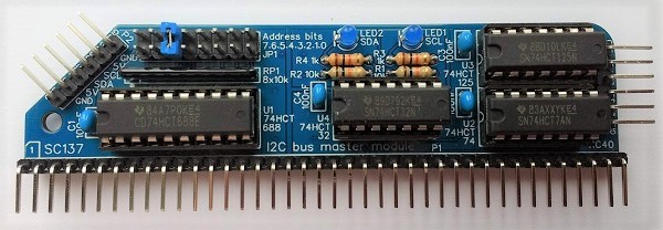
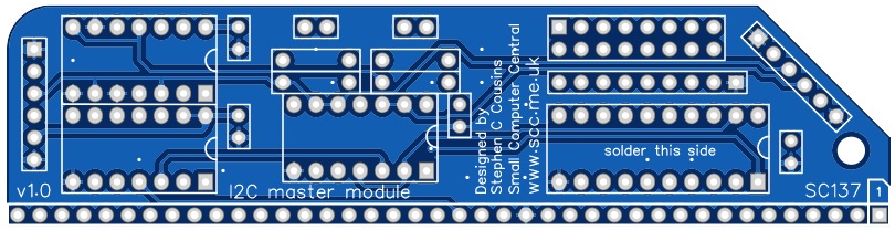
SC137 is an I2C bus master module designed for the RC2014 bus.
Suppliers
| Kits | Website | From | Currency |
| Small Computers Direct | SCDirect | UK | GBP |
| Stephen C Cousins | Tindie | UK | USD |
| PCBs | Website | From | Currency |
| Small Computers Direct | SCDirect | UK | GBP |
| Stephen C Cousins | Tindie | UK | USD |
| Assembled and Tested | Website | From | Currency |
| Not available | |||
| Components | |||
| See parts list |
Description
An I2C bus master is a device that can control I2C slave devices on an I2C bus. This makes the module useful for interfacing with external electronics. In this case, the module generates the I2C bus signals using big-bang code.
The main features of this design are:
- I2C bus master
- LEDs to indicate activity on the SCL and SDA lines
- Simple access using a dedicated I/O port
- Two connections for I2C bus devices
- Supports I2C clock stretching
- Low profile RC2014 style design
User guide
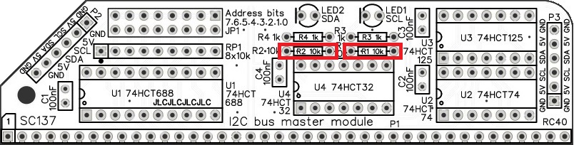
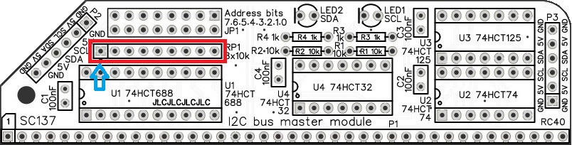
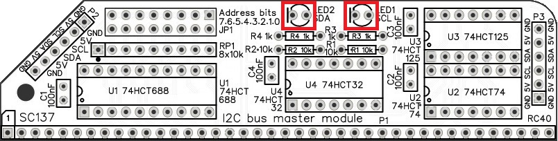
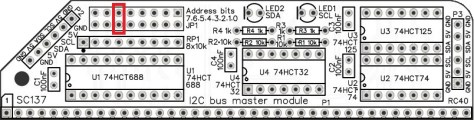
The port address is set with jumper shunts which are fitted to the header pins indicated below.
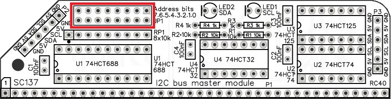
The address selection header is a block of 2 rows of 8 pins. These are the 8 address select jumpers and are labelled with their bit numbers.
The module responds to addresses matching the address set with these jumpers. When a jumper shunt is fitted, that bit must be a 1 (high voltage). When the shunt is not fitted, that bit must be a 0 (low voltage).
If, for example, you wish to set the module to address 32 decimal, which is hexadecimal 20 or binary 00100000, then fit a single jumper shunt to bit 5, as illustrated below.
The default address for an RC2014 is hexadecimal 20, binary 00100000. Note, some systems, such as SC126, use the address 12 decimal, which is hexadecimal 0C or binary 00001100. Check software settings before assuming the address being used.
Software
Example source code can be found here.
Parts list
| Reference | Qty | Component |
| PCB | 1 | SC137, v1.0, PCB |
| C1 to C4 | 4 | Capacitor, ceramic, 100 nF |
| JP1 | 1 | Header, male, 2 x 8 pin, angled, or Header, male, 2 x 8 pin, straight |
| Jumper shunts | 8 | Jumper shunt |
| LED1 and LED2 | 2 | LED, blue, 3mm |
| P1 | 1 | Header, male, 1 x 40 pin, angled |
| P2 and P3 | 2 | Header, male, 1 x 6 pin, angled |
| R1 and R2 | 2 | Resistor, 10k, 0.25W |
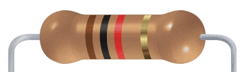
| R3 and R4 | 2 | Resistor, 1k, 0.25W |
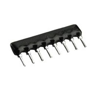
| RP1 | 1 | Resistor pack, 8 x 10k, SIL, 9-pin |
| IC socket 20-pin U1 | 1 | 20-pin PDIP socket |
| IC socket 14-pin U2 to U4 | 3 | 14-pin PDIP socket |
| Integrated circuits | ||
| U1 | 1 | 74HCT688 |
| U2 | 1 | 74HCT74 |
| U3 | 1 | 74HCT125 |
| U4 | 1 | 74HCT32 |
Printed Circuit Board

| Links |
| SC137, v1.0, PCB only (Tindie) |
| SC137, v1.0, Complete kit (Tindie) |
| SC137, v1.0, PCB design files (OSHWLab) |
| SC137, v1.0, Gerber files (ZIP) |
Assembly Guide
Experienced builders can just go ahead and populate the board. There shouldn’t be any surprises to catch you out.
Introduction
This guide assumes you are familiar with assembling circuit boards, soldering, and cleaning. If not, it is recommended you read some of the guides on the internet before continuing.
First check you have all the required components.
Before assembling it is worth visually inspecting the circuit board for anything that looks out of place, such as mechanical damage or apparent manufacturing defects.
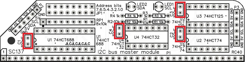
If you have a multimeter that measures resistance or has a continuity test function, check there is not a short on the power supply tracks. Connect the probes to each terminal of one of the capacitors, such as C1. This should be an open circuit, not a short.
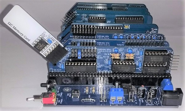
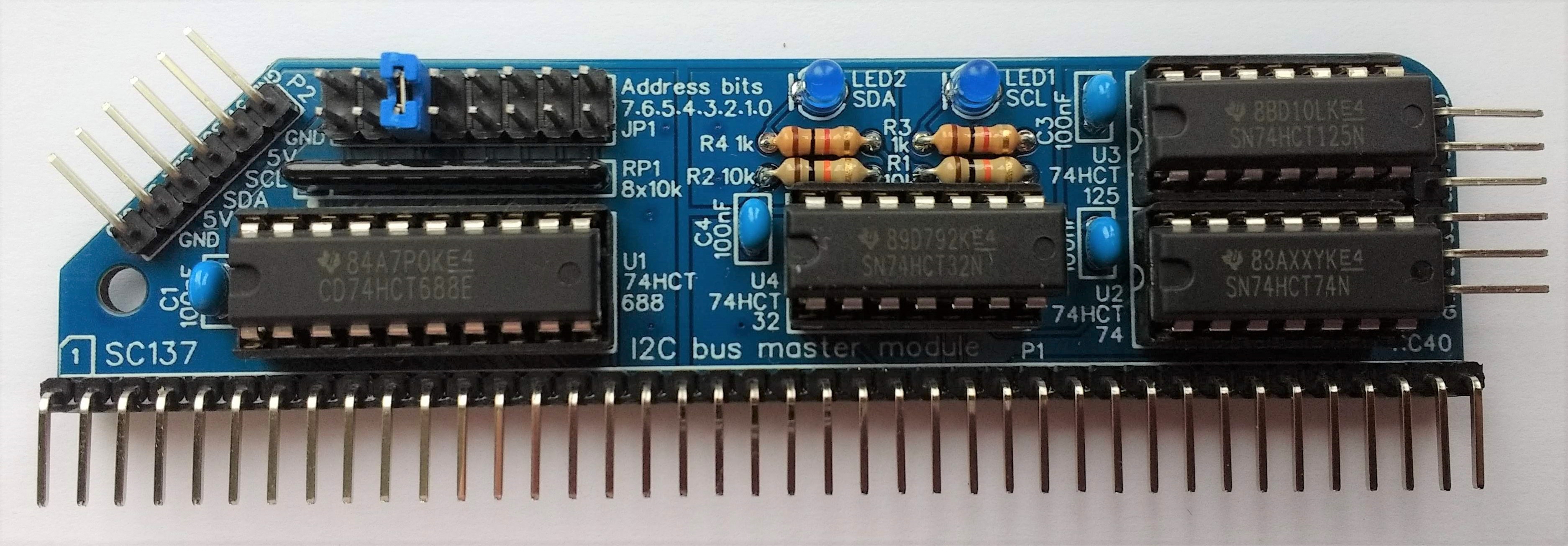
The picture below shows what a completed SC137, I2C bus master module should look like.
Resistors 10k
Fit and solder the 10k resistors R1 and R2 (shown below in red).
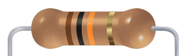
Resistors can be fitted either way around, as they are not polarity dependent.
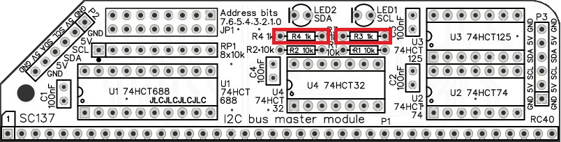
Resistors 1k
Fit and solder the 1k resistors R3 and R4.
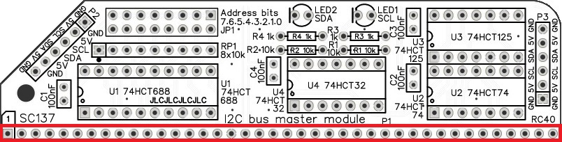
Bus connector
Fit and solder the bus header pins P1.
I2C port connectors
Fit and solder the I2C port connectors P2 and P3.

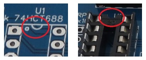
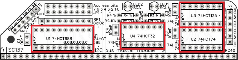
IC sockets
Fit and solder the IC sockets U1 to U4.
Be sure to fit them with the notch matching the legend on the circuit board, so you do not end up fitting the IC the wrong way around too.
Capacitors 100 nF (0.1 µF)
Fit and solder 100nF capacitors C1 to C4.
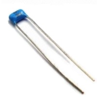
These capacitors can be fitted either way around, as they are not polarity dependent.
The exact value of this component is not critical. The use of very cheap capacitors within the range of about 30 to 200 nF is acceptable.
Resistor network
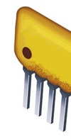
Fit and solder the 8x10k resistor network RP1.
The 10k network will be marked 103.
Take care to fit the resistor network the correct way around. Pin 1 is usually marked with a dot. This end is indicated on the PCB and on the illustration below.
Light Emitting Diodes (LEDs)
Fit and solder the LEDs (LED1 and LED2).
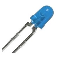
It is important to fit the LEDs the correct way around. LEDs usually have a small flat side to indicate the cathode (the negative end). This should be positioned to match the flat side shown on the circuit board (illustrated to the right). Also, the cathode pin on the LED is usually shorter than the other pin (the Anode).

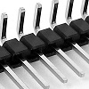
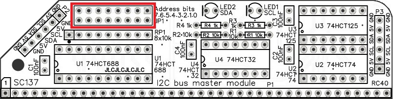
Header (double row)
Address selection is via jumper shunts fitted to a double row of header pins. These can either be straight pins or angled pins. Angled pins stick out above the module allowing easy access to the jumper shunts when the module is fitted to a backplane. Straight pins look neater but do not allow the address to be changed when the module is fitted in a backplane with another module immediately in front of it.
Fit and solder the double row straight or angled header pins, JP1.
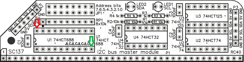
Quick Test
Repeat the check made earlier for a short on the power supply tracks. Connect the meter probes to IC U1 pin 20 (shown below in red) and U1 pin 10 (shown in green). This should not be a short circuit. A reading of more than 1 kΩ (1000 ohms) is acceptable.
Inspection
Remove any solder ‘splats’ with a brush, such as an old toothbrush.
Visually inspect the soldering for dry joints and shorts.
Clean the flux off with suitable cleaning materials.
Visually inspect again.
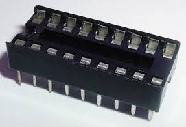
Integrated Circuits
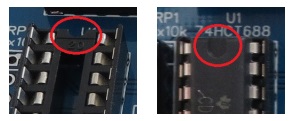
If all the above tests check out okay, insert the integrated circuits into their sockets. Take care to insert them the right way around, as illustrated below. Be careful not to bend any legs over.
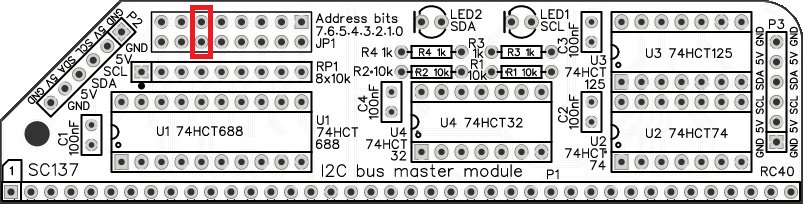
Address select jumpers
Header JP1 is a block of header pins with 2 rows of 8 pins. These are the 8 address select jumpers and are labelled with their bit numbers.
The module responds to addresses matching the address set with these jumpers. When a jumper shunt is fitted, that bit must be a 1 (high voltage). When the shunt is not fitted, that bit must be a 0 (low voltage).
If, for example, you wish to set the module to address 32 decimal, which is hexadecimal 20 or binary 00100000, then fit a single jumper shunt to bit 5 (as illustrated below).
You are now ready to give it a try.
Set the module’s address by fitting a jumper shunt in the position illustrated above.
Testing reset
Connect the I2C bus master module (SC137) to an RC2014 or compatible system and power up.
If your system has a working power on reset then both the module’s LEDs should be off. If your system usually needs a manual reset then reset it now and check both the module’s LEDs are turned off.
If either of the LEDs is turned on at reset, check for a problem around IC U2. If that does not identify the problem, look around U3 and U4.
Testing
The I2C SCL and I2C SDA signals can be tested from BASIC or from the Small Computer Monitor. With the module’s address set to hexadecimal 20 (decimal 32, binary 00100000) the following tests can be performed.
From BASIC:
Enter the lines below, shown in bold, followed by the ENTER key.
PRINT INP(32) AND (128+1)
The number ‘129’ should be displayed, indicating the SDA signal (bit 7) is high and the SCL signal (bit 0) is high. This is the state the two signals should be in following a hardware reset. As the SDA and SCL signals are active low, both LEDs should be off.
OUT 32, 0+1
The SDA LED (bit 7) should be turned on (low) and the SCL LED (bit 0) should be turned off (high).
PRINT INP(32) AND (128+1)
The number ‘1’ should be displayed, indicating the SDA signal (bit 7) is low and the SCL signal (bit 0) is high.
OUT 32, 128+0
The SDA LED (bit 7) should be turned off (high) and the SCL LED (bit 0) should be turned on (low).
PRINT INP(32) AND (128+1)
The number ‘128’ should be displayed, indicating the SDA signal (bit 7) is high and the SCL signal (bit 0) is low.
OUT 32, 128+1
The SDA LED (bit 7) should be turned off (high) and the SCL LED (bit 0) should be turned off (high).
PRINT INP(32) AND (128+1)
The number ‘129’ should be displayed, indicating the SDA signal (bit 7) is high and the SCL signal (bit 0) is high.
From SCM:
Enter the lines below, shown in bold, followed by the ENTER key.
I 20
Note: The first character is the letter “I”.
Typically this will display ‘F9’. Only the state of bit 7 and bit 0 are significant. This should indicate the SDA signal (bit 7) is high and the SCL signal (bit 0) is high. This is the state the two signals should be in following a hardware reset. As the SDA and SCL signals are active low, both LEDs should be off.
O 20 1
Note: The first character is the letter “O”.
The SDA LED (bit 7) should turn on (low) and the SCL LED (bit 0) should be off (high).
I 20
The value displayed should confirm bit 7 is low and bit 0 is high.
O 20 80
The SDA LED (bit 7) should turn off (high) and the SCL LED (bit 0) should be on (low).
I 20
The value displayed should confirm bit 7 is high and bit 0 is low.
O 20 81
The SDA LED (bit 7) should turn off (high) and the SCL LED (bit 0) should be off (high).
I 20
The value displayed should confirm bit 7 is high and bit 0 is high.
Notes
- This design is made in accordance with the “designed for RC2014” labelling scheme.
- RC2014 is a trademark of RFC2795 Ltd.
- This product is designed for hobby use and is not suitable for industrial, commercial or safety-critical applications.
- The product contains small parts and is not suitable for young children.
