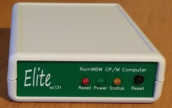
SC131 is a pocket-sized Z180 RomWBW CP/M computer.
- SC131 – Assembly Guide
- SC131 – Circuit Explained
- SC131 – Firmware, RomWBW_SCZ180_131
- SC131 – Firmware, SCM S6
- SC131 – Parts list
- SC131 – Printed circuit board
- SC131 – Software, RomWBW
- SC131 – Support
- SC131 – Troubleshooting
- SC131 – User guide
Downloads
Contributions
- Video: Jazzy Jane: Building SC131 (pocket computer)
- Blog: Johan van Dijk: Build experience of the SC131
Suppliers
| Kits | Website | From | Currency |
| Small Computers Direct | SCDirect | UK | GBP |
| Stephen C Cousins | Tindie | UK | USD |
| Small Computer Central | Lectronz | UK | Euro |
| PCBs | Website | From | Currency |
| Small Computers Direct | SCDirect | UK | GBP |
| Stephen C Cousins | Tindie | UK | USD |
| Small Computer Central | Lectronz | UK | Euro |
| Assembled and Tested | Website | From | Currency |
| Not available | |||
| Components | |||
| See parts list |
Lectronz does collect EU VAT for orders up to 150 EUR
Description
SC131 is a pocket-sized Z180 computer running RomWBW CP/M.
The SC131 PCB can be enclosed in a Hammond 1593N case or used naked.
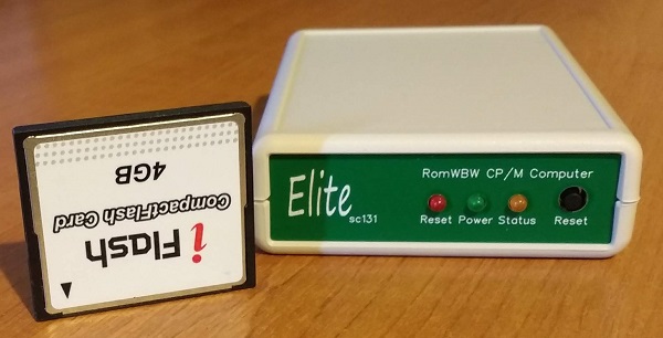
File storage is provided by a Micro SD card which is accessible from the rear of the case.

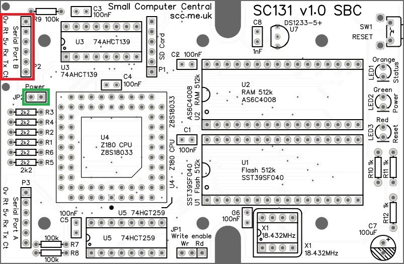
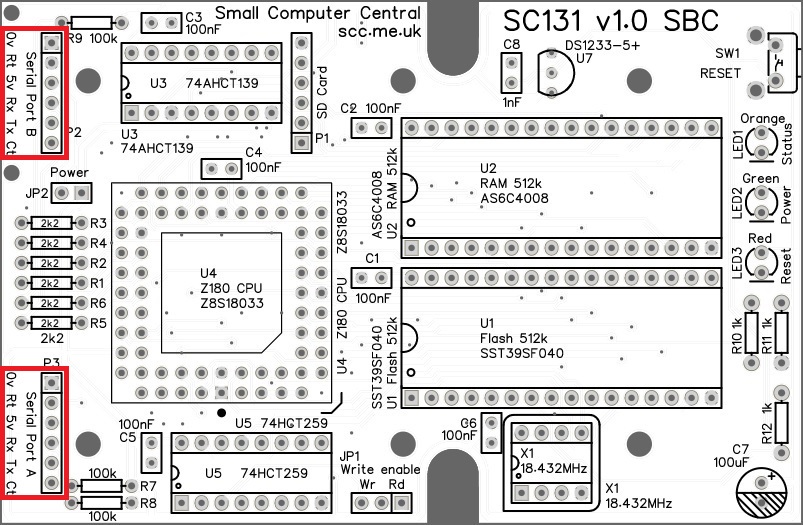
SC131 includes two 5-volt asynchronous serial ports which are accessible from the rear of the case.
Hardware features
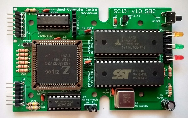
- 1 x Z180 processor clocked at 18.432 MHz.
- 1 x 512k byte RAM.
- 1 x 512k byte Flash (ROM), typically containing RomWBW.
- 2 x Serial ports, asynchronous, 5-volt, with software selectable baud rates.
- 1 x SPI port, primarily for SD card mass storage.
- 1 x Power LED.
- 1 x Status LED.
- 1 x Reset LED.
- 1 x Voltage supervisor and reset device (DS1233).
- 1 x Push button reset switch.
- Printed circuit board size 101.6 mm x 66.14 mm.
- The case measures 111 mm x 75 mm x 25 mm.
Software support
- RomWBW, configuration SCZ180_sc131. This configuration supports an SD card for mass storage.
RomWBW is the primary OS for SC131, providing a robust CP/M implementation.
Design options
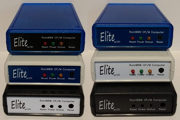
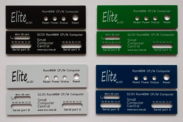
SC131 is available in a number of different designs.
User Guide
SC131 is a Z180 based pocket-sized retro computer.
SC131 normally has Flash memory containing RomWBW in socket U1.
Quick Guide to Jumpers
As a quick guide to getting started: Fit a jumper shunt in the position shown below.
And for those who are sensible enough to read User Guides…
Power
The power required for this board is 5 V D.C. at 100 mA without an SD card or other accessories. With an SD card present the current requirement could rise to 300 mA.
SC131 is normally powered from the primary serial port (serial port A).
SC131 is typically connected to a computer or terminal with an FTDI style serial adapter. This adapter also provides power for the SC131. It is vital that the adapter is able to provide enough power without the voltage dropping significantly. If SC131’s red reset LED stays on it is likely due to the voltage supervisor (U7) holding the processor in reset because the voltage reaching the board is not adequate.
The board can also be powered from the serial port B. This requires a jumper shunt fitted to JP2 to connect power from serial port B.
WARNING: You should normally only connect one power source to the system at a time.
As power can flow either way, the jumper (JP2) also enables serial devices to be powered from SC131. If such a device is used in serial port B, fit a jumper shunt to JP2.
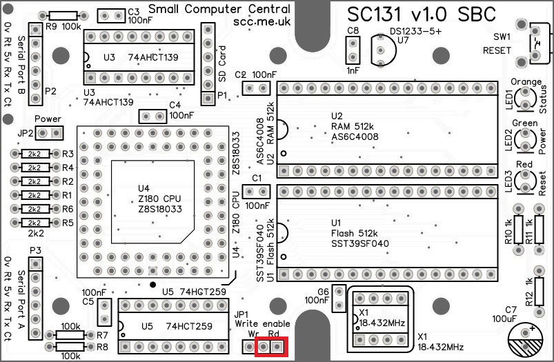
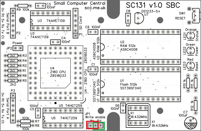
Write Protect Flash
Jumper JP1 enables the Flash chip to be write protected. It is unlikely the Flash chip will be corrupted in normal operation due to the software requirements to write to it. However, for peace of mind you can disable writing with a jumper shunt.
Fit the shunt in the “Rd” (read only) position shown below in green to disable writing (to write protect the Flash memory). Alternatively, fit the shunt in the “Wr” (write enabled) position shown below in red to enable writing.
Serial Ports
The motherboard has two asynchronous serial ports, with software selectable baud rate. These are 5 volt FTDI style ports.
The pin-out, below, describes signals with respect to SC131, so an output is a signal from the SC131 to a computer or terminal.
| Pin | Function |
| 1 | Ground (GND) |
| 2 | Request To Send (RTS) output |
| 3 | Vcc (5V) |
| 4 | Recieve Data (RxD) input |
| 5 | Transmit Data (TxD) output |
| 6 | Clear To Send (CTS) input |
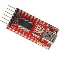
A typical FTDI style serial adapter is illustrated to the right.
This is fitted to the serial port by a 6-way Dupont cable.
The default serial ports settings are as follows:
| Setting | RomWBW |
| Baud rate | 115200 |
| Data bits | 8 |
| Parity | none |
| Stop bits | 1 |
| Flow control | Hardware (recommended) |
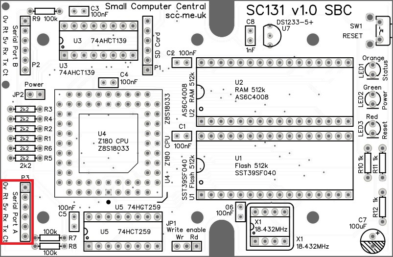
The default serial port connection is P3, Serial Port A.
SPI Port
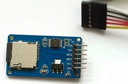
SC131 has an SPI port, primarily for the connection of a Micro SD card adapter.

The signals are 5 volt levels, with the following pin-out.
| Pin | Function |
| 1 | Chip select (active low) |
| 2 | Clock |
| 3 | Master out, slave in |
| 4 | Master in, slave out |
| 5 | Vcc (5V) |
| 6 | Ground (GND) |
A typical micro SD card adapter is illustrated to the right.
This may be fitted directly to the circuit board (when installed in the recommended case) or by a 6-way cable (if required).
Memory Map
The physical memory map is simply 512k byte of Flash ROM at the bottom of memory and 512k bytes of RAM at the top of memory.
The Z180’s memory management unit deals with mapping chunks of this memory into the logical 64k memory map supported by the Z80/Z180 instruction set.
| Address | Function |
| 0x80000 to 0xFFFFF | RAM (512k bytes) |
| 0x00000 to 0x7FFFF | Flash ROM (512k bytes) |
Input / Output Ports
The SC131’s I/O port addresses are as follows.
| Address | Function |
| 0xC0 to 0xFF | Z180’s internal I/O registers |
| 0x0E (0b00X0XX1X) | Status LED port (write only) Bit 2 = LED control (active low) |
| 0x0C (0b00X0XX0X) | SPI device select (write only) Bit 2 = SPI select (active low) |
As SC131’s does not provide expansion through an accessible processor bus, there is no need for tight I/O address decoding. The address values in brackets, in the table above, are the binary addresses that each device can be accessed, where ‘X’ is either a high or a low bit. The hexadecimal addresses, not in brackets, are the addresses software should use.
The status LED is initially turned on but is otherwise free to use. The LED can be written to with output statements or instructions.
- Turn the status LED off from BASIC:
- OUT 14, 255
- Turn the status LED on from BASIC:
- OUT 14, 0
Note that the LED is turned on by writing a 0 (not a 1). This is because the LED output is active low. This is necessary to allow the LED to be turned on by a hardware reset. The reset signal clears the output latch to zero, thus zero is the on state.
Parts List
| Reference | Qty | Component |
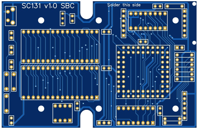
| PCB | 1 | SC131, v1.0, PCB |
| C1 to C6 | 6 | Capacitor, ceramic, 100 nF |
| C7 | 1 | Capacitor, electrolytic, 100 µF |
| C8 | 1 | Capacitor, ceramic, 1 nF |
| JP1 | 1 | Header, male, 1 row x 3 pin, straight |
| JP2 | 1 | Header, male, 1 row x 2 pin, straight |
| Jumper shunts | 2 | Jumper shunt |
| LED1 | 1 | LED, orange, 3mm |
| LED2 | 1 | LED, green, 3mm |
| LED3 | 1 | LED, red, 3mm |
| P1 | 1 | Header, female, 1 row x 6 pin, straight |
| P2 and P3 | 2 | Header, male, 2 row x 6 pin, angled |
| R1 to R6 | 6 | Resistor, 2k2, 0.25W |
| R7 to R9 | 3 | Resistor, 100k, 0.25W |
| R10 to R12 | 3 | Resistor, 1k, 0.25W |
| SW1 | 1 | Switch, tactile button, angled |
| U1 | 1 | SST39SF040, 512k byte Flash |
| U2 | 1 | AS6C4008, 512k byte SRAM |
| U3 | 1 | 74AHCT139 |
| U4 | 1 | Z8S180 CPU (PLCC 68 pin) Z8S18020VSC, or Z8S18020VSG, or Z8S18033VSC, or Z8S18033VSG |
| U5 | 1 | 74HCT259 |
| U7 (no U6!) | 1 | DS1233-5+ EconoReset |
| X1 | 1 | Oscillator, 18.432 MHz |
| IC socket 8-pin X1 | 1 | 8-pin PDIP socket (not included in kit) |
| IC socket 16-pin U3 and U5 | 2 | 16-pin PDIP socket |
| IC socket 32-pin U1 and U2 | 2 | 32-pin PDIP socket |
| IC socket 68-pin U4 | 1 | 68-pin PLCC socket |
| LED former | 1 | Header, male, 2 row x 8 pin, angled |
| Micro SD card adapter | ||
| Micro SD adapter | 1 | Micro SD card adapter |
| Standoffs | 2 | Standoff, M2 x 10 mm |
| Screws | 4 | Machine screw, M2 x 6 mm |
| Case parts | ||
| Case | 1 | Hammond 1593N |
| PCB screws | 3 | Self-tapping screw #4 x 0.25″ |
| Front panel | 1 | Font panel |
| Back panel | 1 | Back panel |
Printed Circuit Board

| Supplier | Website | Ships from |
| Stephen C Cousins | Tindie | UK |
| pcb4diy | eBay | Germany |
| pcb4diy | pcb4diy.de | Germany |
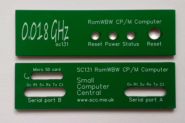
In addition to the main PCB, the cased SC131 has front and back panels made from printed circuit board material. These are available in a range of colours and with a choice of logos. As the designs are available at EasyEDA.com you can easily produce custom panels with your own legend.
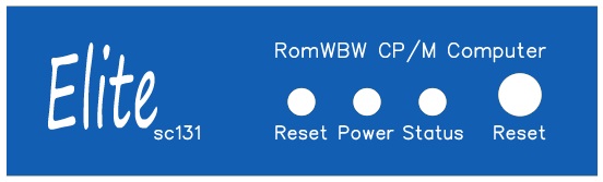
Front Panel: Elite
| Links |
| SC131 Front Elite, v1.1A, PCB design files (EasyEDA) |
| SC131 Front Elite, v1.1A, Gerber files (ZIP) |
| Supplier | Website | Ships from |
| Stephen C Cousins | Tindie | UK |
| pcb4diy | eBay | Germany |
| pcb4diy | pcb4diy.de | Germany |
Front Panel: 0.018 GHz
| Supplier | Website | Ships from |
| Stephen C Cousins | Tindie | UK |
| pcb4diy | eBay | Germany |
| pcb4diy | pcb4diy.de | Germany |

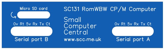
Back Panel
| Supplier | Website | Ships from |
| Stephen C Cousins | Tindie | UK |
| pcb4diy | eBay | Germany |
| pcb4diy | pcb4diy.de | Germany |
Circuit Explained
The SC131, pocket-sized Z180 computer includes the following:
- Z180 8-bit CPU
- One 512k byte static RAM chip
- One 512k byte Flash ROM chip
- Two 5 volt FTDI style asynchronous serial ports
- One 5 volt SPI / SD Card port
- Clock oscillator (18.432 MHz)
- Three LEDs: power, status, reset
- Power supply supervisor and a reset circuit
- Power input (5 volt, typically 100 mA, max. 300 mA)
C1 to C6
These capacitors provide power supply decoupling (or bypass). The fast switching in digital circuits creates spikes on the power supply lines which are suppressed with decoupling capacitors placed at key points on the circuit board.
The exact value of this component is not critical. The use of very cheap capacitors within the range of about 50 to 150 nF is acceptable.
C7
This capacitor provides additional support for transient current demands.
C8
This capacitor is required by the Voltage Supervisor and Reset device (DS1233-5+, U7) when an external reset switch and pull-up resistor are connected to the reset line. See DS1233-5+ datasheet for more details.
The exact value of this component is not critical. The datasheet for the DS1233 specifies a value from 0.5 to 10 nF, thus a very low cost component with a wide tolerance is acceptable.
JP1
Jumper 1 allows Flash chip U1’s write enable input to be connected to either Vcc (5 volts) or the CPU’s write output (/WR).
When the Flash chip’s write enable input is connected to Vcc, the Flash chip will never get a write enable signal and thus the memory is protected against being changed. When connected to the CPU’s write output, it is possible to write to the Flash chip.
Writing to the Flash chip is unlikely to happen by accident due to the software requirements. However, for peace of mind it is generally best to disable writing with this jumper.
JP2
Jumper 2 allows the main board to be powered from serial port B. It also allows main board to power a peripheral connected to serial port B.
Normally power is supplied from serial port A but there may be cases when power should be provided from serial port B. In these cases, a jumper shunt should be fitted to JP2.
Power should normally only be supplied from one source at a time, so take this into account when using this jumper.
LED1
The orange LED is used to indicate the system’s status. At reset the LED is turned on by hardware but after that it is software controlled. Using the current version of RomWBW the LED remains on until the user makes a selection from the start-up menu, then it is used to indicate activity on the SD card.
LED2
The green LED is used to indicate the presence of the 5 volt supply.
LED3
The red LED indicates the system is being held in reset. It should come on for about half a second at power up or when the reset button is pressed.
If it stays on then the likely cause is inadequate supply voltage. The system includes a voltage supervisor and reset device (U7). This device provides a clean reset and also monitors the supply voltage. If the supply voltage is lower than about 4.7 volts it holds the system in reset. This ensures the system only runs when the supply is adequate for reliable operation.
As the system is normally powered from a USD to serial adapter, it is vital the adapter be capable of supply up to 300 mA without dropping the voltage below about 4.7 volts. Even some branded adapters may not meet this requirement.
P1
This connector gives access to the 5 volt SPI port. This port uses the Z180’s hardware clocked serial I/O for high speed interfacing.
| Pin | Function |
| 1 | Chip select (active low) |
| 2 | Clock |
| 3 | Master out, slave in |
| 4 | Master in, slave out |
| 5 | Vcc (5V) |
| 6 | Ground (GND) |
This connector is not accessible from outside the cased version of SC131 and is placed specifically to mount a Micro SD card adapter.
P2 and P3
Serial ports A and B are connected via P2 and P3. These are FTDI style 5 volt serial ports. Port A includes RTS/CTS flow control signals, while port B does not.
| Pin | Function |
| 1 | Ground (GND) |
| 2 | Request To Send (RTS) output from Z180 |
| 3 | Vcc (5V) |
| 4 | Recieve Data (RxD) input to Z180 |
| 5 | Transmit Data (TxD) output from Z180 |
| 6 | Clear To Send (CTS) input to Z180 |
R1 to R6
These provide current limiting between the Z180 system and the serial devices on serial ports A and B, providing protection for when one is powered and the other is not.
R7 to R9
The resistors provide pull up and pull down for the serial port inputs, thus holding them in known states when no device is connected.
R10 to R12
These are the current limiting resistors for the LEDs.
SW1
This tactile button grounds the reset signal, resetting the system.
U1
This is a 512k byte Flash memory chip. This holds the board’s firmware, typically RomWBW.
U2
This is a 512k byte static RAM chip. This is used to store the program and data being worked on at the current time.
U3
The 74AHCT139 is the addresses decoder, providing chip enable signals for the three memory chips. It is a dual 2-to-4 line decoder. One decoder is used to select between the RAM and the Flash memory chips. The other forms part of the address decoding for input/output devices.
Memory: Inputs are memory request (MREQ) and A19. Memory request is low when memory is being accessed and A19 determines if it is Flash memory (A19 low) or RAM (A19 high).
Input/output: This provides a partially decoded I/O device enable. An I/O address of b00XXXXXX results in its output Y0 going low, where ‘X’ indicates an address bit in either state.
U4
This is a 68-pin PLCC packaged Z8S180 CPU. It must be rated at a frequency at least as high as the clock signal PHI.
PHI is initially the oscillator (X1) frequency divided by 2, as the Z180 turns on its clock divider at reset. However, current firmware turns this off, so PHI is then equal to the on-board oscillator (X1) frequency.
U5
This is a 74HCT259 addressable latch. This is enabled by the partially decoded I/O address from U3. Two of the output latches are used: one for the status LED and the other to enable the SPI device (in this case a micro SD card).
As this design does not have an accessible bus for expansion, there is no need to fully decode the I/O addresses. The SPI enable address is 0b00XX0XX0X, while the LED address is 0b00X0XX1X. The convention is to use address 0x0C for the SPI enable and 0x0E for the LED.
In both cases, when an I/O write is performed the state of data bit 2 is latched to the specified output. The SPI enable is an active low signal. Similarly, the LED output is active low, so it must be set low to turn the LED on.
U6
There is no U6!
U7
This is a DS1233-5+ voltage supervisor and reset device. It provides a clean, reliable reset for the Z180 system. The device pulls the system’s reset signal low when the supply voltage is less than about 4.7 volts. If your system does not run, check the supply voltage and the reset signal.
The reset line can also be pulled down by the reset button. The DS1233 senses this and pulls its own output low to provide a clean reset pulse. This eliminates the typical switch bounce that could lead to reliability problems.
X1
This oscillator provides the CPU’s main 18.432 MHz clock. This is the frequency required when running the board with current firmware.
Notes
- This product is designed for hobby use and is not suitable for industrial, commercial or safety-critical applications.
- The product contains small parts and is not suitable for young children.
- RomWBW has been provided free of charge by its author Wayne Warthen.
