SC102 is a very flexible Z80 CTC module designed for the RC2014 bus.
A later design is now available: SC718

Documentation
- SC102 – Description
- SC102 – Assembly Guide
- SC102 – Circuit Explained
- SC102 – Fault Finding
- SC102 – Parts List
- SC102 – Printed Circuit Board
- SC102 – User Guide
- SC102 – PCB design files v1.1 (EasyEDA)
Downloads
Suppliers
| Kits | Website | From | Currency |
| Small Computers Direct | SCDirect | UK | GBP |
| Stephen C Cousins | Tindie | UK | USD |
| Small Computer Central | Lectronz | UK | Euro/USD |
| PCBs | Website | From | Currency |
| Small Computers Direct | SCDirect | UK | GBP |
| Stephen C Cousins | Tindie | UK | USD |
| Small Computer Central | Lectronz | UK | Euro/USD |
| Assembled and Tested | Website | From | Currency |
| Not available | |||
| Components | |||
| See parts list |
Tindie does not collect VAT for EU countries
Lectronz does collect EU VAT for orders up to 150 EUR
Examples
Older Versions
Description
I’ve only designed a few printed circuit boards in my life, and the most recent of those was about 26 years ago. So my Z80 CTC module for the RC2014 is the first board I’ve designed in a while and the first with modern tools.

The main features of this module are:
- Full Z80 mode 2 interrupt support (IEI/IEO daisy-chain)
- Software control of the baud rate for SIO port B
- Timer and clock tick interrupt
- Source of bus clock (option) to potentially reduce board count
- On-board clock option to make it independent of the CPU clock
- Interrupt mode 2 converter for up to 4 devices
User Guide
The Z80 CTC module (SC102) provides four programmable counter/timers with very flexible input and output connectivity, as well as support for Z80 mode 2 interrupt daisy chaining.
All four channels have an external clock/trigger input, and the first three channels have a zero count/time-out output. All of these signals are available on a connector at the back of the board. Each counter/timer channel can be started as a timer by an external trigger signal on the channel’s input.
Each counter/timer channel can count down, from a pre-set value, each time the selected edge (rising or falling) occurs on its input. When the counter reaches zero a pulse appears on the channels output, the counter is automatically reloaded and an optional interrupt is generated.
Feeding a clock signal to a channel input enables the module to generate a periodic tick signal and/or interrupt. Jumper options allow each channel to be optionally supplied with a clock signal from one of these sources:
- RC2014 bus primary clock (CLK)
- RC2014 bus secondary clock (CLK2)
- The module’s on-board oscillator output (CLKX)
- RC2014 bus USER pin (USER 5, 6, 7, 1 for CTC channels 0, 1, 2, 3)
- An external signal from a connector on the back edge of the module
The first three channels can each act as a baud rate generator by generating a periodic output at the required frequency, as described above. Any one of these can be set to output a baud rate clock to the RC2014 secondary clock (CLK2).
By pre-setting a channel’s counter to 1 the module can generate a Z80 mode 2 interrupt each time the selected edge occurs on the channel’s input. This allows the module to act as a four channel Z80 mode 2 interrupt controller for non-Z80 devices.
For full details of the Z80 CTC see the Zilog data sheet.
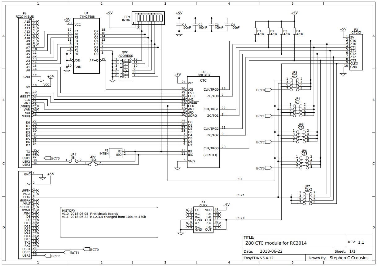
Schematic
Errata
Version 1.0 of the schematic and PCB label resistors R1, R2, R3 and R4 as 100k, but it was found that if all four inputs were set to the RC2014 bus primary clock (CLK) the system would become unreliable. The value has therefore been changed to 470k to reduce loading of the clock signal.
Configuring the CTC Module
The following are just a few examples of how you can configure and use the CTC module. To realise its full potential it is necessary to study the Zilog Z80 CTC data sheet, which can be found on the internet by searching for “zilog UM0081”.
Most of the following examples require software support.
CTC Module as the Primary Clock
The CTC module can provide a clock source for the RC2014 bus primary clock (CLK). This means a separate clock module is not required, potentially saving one backplane slot.
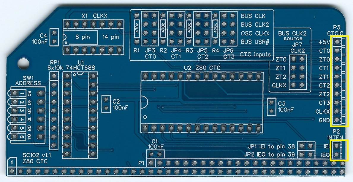
The illustration below shows the jumper shunt positions required to link the output of the on-board oscillator to the RC2014 bus primary clock (CLK). The illustration uses JP4, but any of the jumpers JP3 to JP6 can be used.

Input
Each channel’s counter/timer input can be either:
- RC2014 bus primary clock (CLK)
- RC2014 bus secondary clock (CLK2)
- The CTC’s on-board oscillator output (CLKX)
- RC2014 bus USER pin (USER 5, 6, 7, 1 for CTC channels 0 to 3)
- An external signal from connector P3
The illustration below shows the jumper shunt positions for:
- Channel 0 to use the RC2014 bus primary clock (CLK) as its input
- Channel 1 to use the RC2014 bus secondary clock (CLK2) as its input
- Channel 2 to use the on-board oscillator clock (CLKX) as its input
- Channel 3 to use the signal on RC2014 bus pin 37 (USER1) as its input

To use the signal on P3’s CT0, CT1, CT2 or CT3 input, just remove the channel’s input jumper shunt so the input is not connected to any of the above.
Output
The outputs from channels 0 to 2 (ZT0, ZT1 and ZT2) are connected to P3, so that they can be easily accessed for any required purpose. Channel 3 does not have an accessible output signal.
In addition, the outputs are connected to jumper JP7, along with the on-board oscillator clock (CLKX). Jumper JP7 enables the RC2014 bus secondary clock (CLK2) to be supplied by any one of the CTC outputs or the on-board oscillator output (CLKX).
By using a CTC output as the secondary clock source, port B of the serial SIO module can have its baud rate controlled by software.
If your RC2014 system already has a device providing the secondary clock signal (CLK2), then do not fit a jumper shunt to JP7.
The illustration below shows the jumper shunt position required to use the output of CTC channel 1 as the source for the secondary bus clock (CLK2).

Baud Rate Generator
For users of the official RC2014 Z80 SIO/2 module, the CTC module can provide a software selectable baud rate clock for SIO port B.
In the example below, the normal clock module is removed and the CTC module provides the RC2014 bus primary and secondary clocks (CLK and CLK2). The primary clock (CLK) is 7.3827 MHz, while the secondary clock (CLK2) is 0.6144 MHz. The primary clock is used by the processor and by SIO port A (115200 baud), while the secondary clock is used by SIO port B (9600 baud).

The jumper shunt positions shown above perform the following functions:
- Red – Sets the RC2014 bus primary clock (CLK) to the CTC module’s on-board oscillator output (CLKX).
- Green – Sets CTC channel 1 clock input to the CTC module’s on-board oscillator output (CLKX).
- Yellow – Links CTC channel 1 output to the RC2014 bus secondary clock line, providing the baud rate clock for SIO port B.
The SIO/2 module’s port B jumper shunt should be removed to isolate port B’s clock from port A’s clock.
To set CTC channel 1 to generate the required 0.6144 MHz clock, issue the following Small Computer Monitor commands:
O 89 55
O 89 6
Or the BASIC commands:
OUT &H89, &H55
OUT &H89, 6
Where:
- &H89 is the address of CTC channel 1’s control register (&H88+1)
- &H55 selects:
- No interrupt
- Counter mode
- Count on rising edge
- Time constant follows
- 6 is the time constant
The time constant value 6 selects divide by 12. The doubling of the divider, or halving of the frequency, is caused by the CTC only counting the second edge.
With the CTC input at 7.3728 MHz and CTC channel 1 set to divide by 12, CTC channel 1 output is 7.3728 / 12 MHz, which is 0.6144 MHz. The 0.6144 MHz clock is output to the RC2014 secondary clock line (CLK2) and is picked up by SIO/2 port B. By default the SIO is set to divide the incoming clock by 64 to generate the baud rate. The baud rate is thus 0.6144 / 64 MHz, which is 0.0096 MHz or 9600 Hz.
Time constant value and baud rates:
| Constant | Baud rate SIO = divide 64 | Baud rate SIO = divide 16 |
| 1 | 57600 | 230400 |
| 2 | 28800 | 115200 |
| 3 | 19200 | n/a |
| 4 | 14400 | 57600 |
| 6 | 9600 | 38400 |
| 12 | 4800 | 19200 |
| 16 | n/a | 14400 |
| 24 | 2400 | 9600 |
| 48 | 1200 | 4800 |
| 96 | 600 | 2400 |
| 192 | 300 | 1200 |
Due to the way the CTC synchronises its counting function to the bus clock, the above only works when the bus clock (CLK) is the same signal as the CTC input.
Cascading Channels
By linking the output of one CTC channel to the input of the next, the two channels can be cascaded to give a greater range.
The illustration below shows the jumper shunt position required to link the output of channel 1 to the input of channel 2.

Interrupt Controller
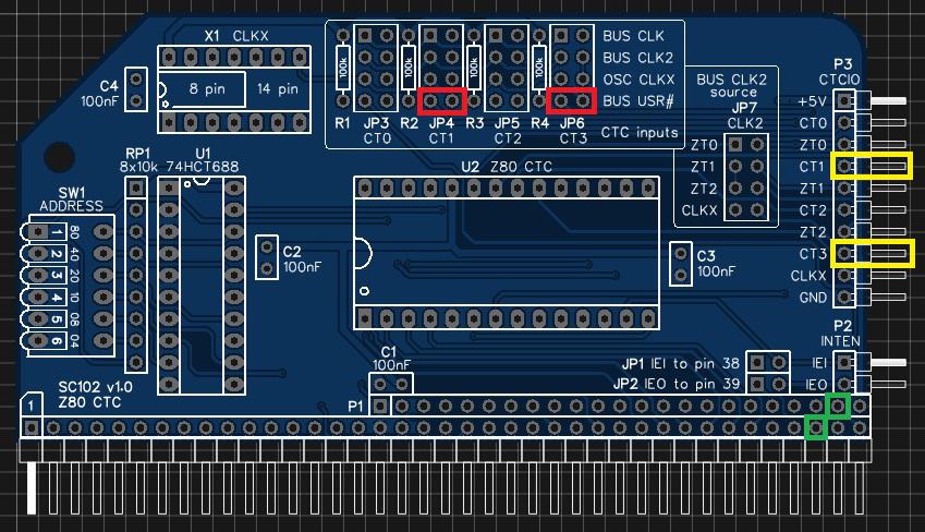
The CTC module can act as an interrupt controller, whereby it provides Z80 interrupt mode 2 functions for up to four devices that do not themselves support mode 2.
The illustration below shows the jumper shunt positions (in red) required to use channel 1 and channel 3 as interrupt controllers for non-mode 2 devices. The interrupt signals from the non-mode 2 devices can be connected to CT1 and CT3 on P3 (shown in yellow) with Dupont wires, or to USER pins on the RC2014 bus (shown in green).
The software will be required to:
- Set the processor to interrupt mode 2 and initialise the I register
- Set the interrupt vector table entries for the CTC’s interrupts
- Set the CTC’s interrupt vector register
- Set the CTC channel(s) to count down from 1
- Set the CTC channel(s) input edge to either rising or falling
- Set the CTC channel(s) to generate an interrupt
- Write an interrupt handler for the non-mode 2 device
Interrupt Daisy Chain
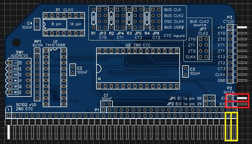
If your system has more than one device using interrupt mode 2, it will be necessary to set up an interrupt daisy chain.
This is fully described in the Z80 peripherals data sheet, but essentially it requires linking the output (IEO) of one interrupt generating device to the input (IEI) of the next, and so on. The position in the chain determines the device’s interrupt priority.
The illustration shows the connections required when using external Dupont wires on P2 (in red) and the RC2014 bus USER pins (in yellow).
Setting up a mode 2 interrupt system is not trivial so requires study of the data sheets rather than following any simple example I could write here.
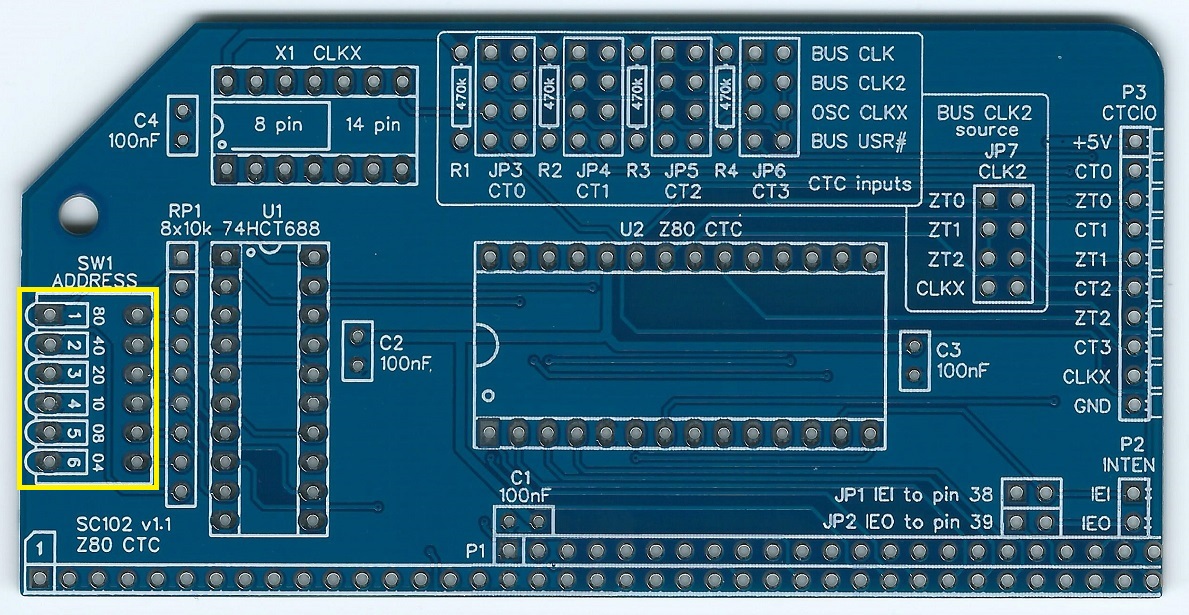
Address Selection
The module’s address can be set to any address that is a multiple of 4, such as address 0, 4, 8, 12, 16, … , 252. This address is known as the base address, with the module occupying this address plus the next three addresses. Thus if the base address is 0, then the module occupies the address range 0 to 3.
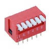
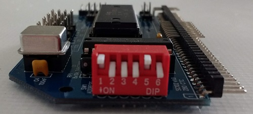
The address is set with the 6 way DIP switch SW1.
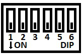
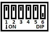
The six address switches, 1 to 6, represent addresses 128, 64, 32, 16, 8 and 4 respectively. The base address is the sum of all the switches in the Off position. For a piano style DIP switch, as illustrated below, Up is Off and Down is On.
In the illustration below the switches are:
Up Down Down Down Up Down
This represents the address:
128 + 0 + 0 + 0 + 8 + 0
= 128 + 8
= 136 (or 0x88 in hexadecimal).

In order to provide some certainty for software it is strongly recommended you set the base address of your first CTC module to 0x88, so that the module occupies I/O addresses 0x88 to 0x8B. This is done by setting the switches as illustrated above.
If you have a second CTC module the recommended base address is 0x8C.
WARNING: The suggested addresses clash with the official RC2014 serial / ACIA module, which does not have tight address decoding. It is assumed that most people wanting a Z80 CTC module will be using a Z80 SIO as the serial device, as the ACIA can not generate Z80 mode 2 interrupts.
If everybody follows these recommendations then software written for the CTC module will know where to find the CTC hardware.
The following table shows examples of address switch settings.
Switch
Address

Recommended 1st CTC
Base address 0x88
Range 0x88 to 0x8B
(136 to 139 decimal)

Recommended 2nd CTC
Base address 0x8C
Range 0x8C to 0x8F
(140 to 143 decimal)
Base address 0x00
Range 0x00 to 0x03
(0 to 3 decimal)

Base address 0x04
Range 0x04 to 0x07
(4 to 7 decimal)

Base address 0x08
Range 0x08 to 0x0B
(8 to 11 decimal)

Base address 0x40
Range 0x40 to 0x43
(64 to 67 decimal)

Base address 0x44
Range 0x44 to 0x47
(68 to 71 decimal)

Base address 0x48
Range 0x48 to 0x4B
(72 to 75 decimal)

Base address 0x4C
Range 0x4C to 0x4F
(76 to 79 decimal)

Base address 0x50
Range 0x50 to 0x53
(80 to 83 decimal)

Base address 0xF0
Range 0xF0 to 0xF3
(240 to 243 decimal)

Base address 0xF4
Range 0xF4 to 0xF7
(244 to 247 decimal)
Base address 0xF8
Range 0xF8 to 0xFB
(248 to 251 decimal)
Base address 0xFC
Range 0xFC to 0xFF
(252 to 255 decimal)
Credits
Thanks to all those who provided encouragement, feedback and contributed ideas to the design. Specifically: Mark T, Tom S, Jon L, Nigel K, Samster, Jay C, Colin L, Karl B, Spencer O, and anyone else I forgot! Also thanks to those who reported errors in this guide, which hopefully I’ve fixed.
See RC2014 google group for full details:
https://groups.google.com/forum/#!topic/rc2014-z80/4s1pwSQoddQ
Parts List
| Reference | Qty | Component |
| PCB | 1 | SC102, v1.1, PCB |
| C1 to C4 | 4 | Capacitor, ceramic, 100 nF |
| JP1 plus JP2 | 1 | Header, male, 2 x 2 pin, straight |
| JP 3 to JP7 | 5 | Header, male, 2 x 4 pin, straight |
| JP1 to JP7 shunt | 7 | Jumper shunt |
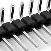
| P1 | 1 | Header, male, 2 x 39 pin, angled |
| P2 | 1 | Header, male, 1 x 2 pin, angled |
| P3 | 1 | Header, male, 1 x 10 pin, angled |
| R1 to R4 | 4 | Resistor, 470k, 0.25W |
| RP1 | 1 | Resistor pack, 8 x 10k, SIL, 9-pin |
| SW1 | 1 | DIP switch, 6 way, piano style |
| U1 | 1 | 74HCT688 |
| U1 socket | 1 | 20-pin DIP socket |
| U2 | 1 | Z80 CTC, Z84C3008PEG |
| U2 socket | 1 | 28-pin DIP socket |
| X1 | 1 | Oscillator 7.3728 MHz |
| X1 socket | 1 | 14-pin PDIP socket (optional) |
Printed Circuit Board
| Supplier | Website | Ships from |
| Stephen C Cousins | Tindie | UK |
| pcb4diy | eBay | Germany |
| pcb4diy | pcb4diy.de | Germany |
Assembly Guide
Experienced builders can just go ahead and populate the board. There shouldn’t be any surprises to catch you out.
This guide assumes you are familiar with assembling circuit boards, soldering, and cleaning. If not, it is recommended you read some of the guides on the internet before continuing.
First check you have all the required components.
Before assembling it is worth visually inspecting the circuit board for anything that looks out of place, such as mechanical damage or apparent manufacturing defects.
If you have a multimeter that measures resistance or has a continuity test function, check there is not a short on the power supply tracks. Connect the probes to each terminal of one of the capacitors, such as C1. This should be an open circuit, not a short.
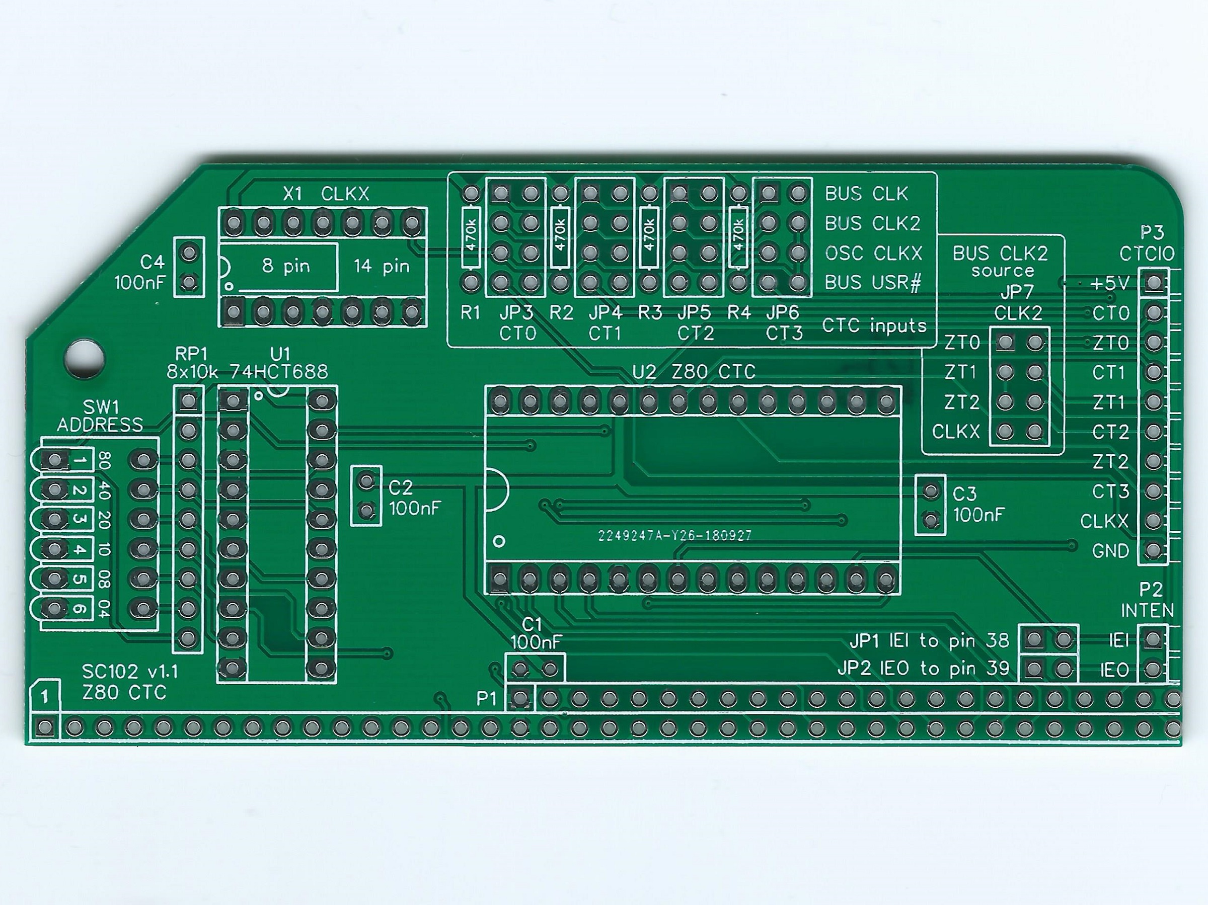
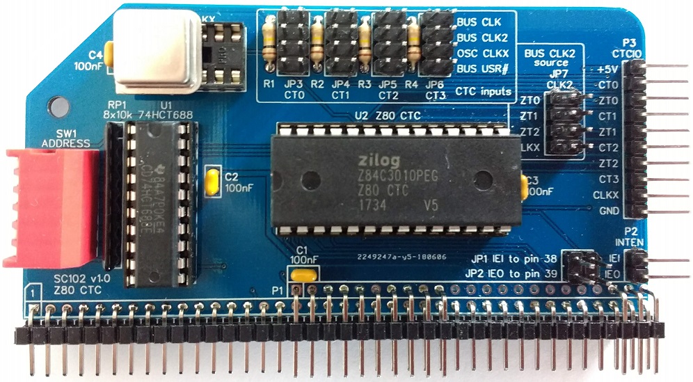
The picture below shows what a completed SC102 Z80 CTC Module should look like.
Version 1.0 of the schematic and PCB label resistors R1, R2, R3 and R4 as 100k, but it was found that if all four inputs were set to the RC2014 bus primary clock (CLK) the system would become unreliable. The value has therefore been changed to 470k to reduce loading of the clock signal.
Resistors
Fit and solder the 470K resistors R1 to R4 (shown in yellow below).

These can be fitted either way round, as they are not polarity dependent.
These should be 470k resistors, not the 100k resistors shown on v1.0 schematic and circuit board.

IC sockets
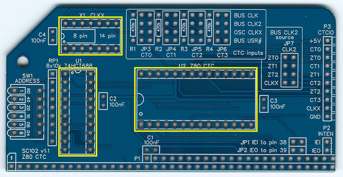
Fit and solder IC sockets for U1, U2, and X1.
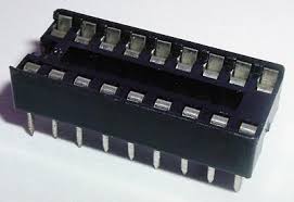
Be sure to fit them with the notch matching the legend on the circuit board, so you do not end up fitting the IC the wrong way round too.
You may wish to solder the oscillator X1 directly to the board, in which case fit the oscillator now instead of the socket. The oscillator can be either the 8-pin or the 14-pin package size. The correct position for each is shown on the circuit board. Pin 1 of the oscillator is normally indicated by a ‘sharp’ corner, while the other three corners are rounded.
The sockets should be fitted in the positions shown below.
Capacitors
Fit and solder capacitors C1 to C4.
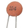
These can be fitted either way round, as they are not polarity dependent.
Resistor Network
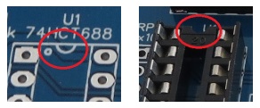
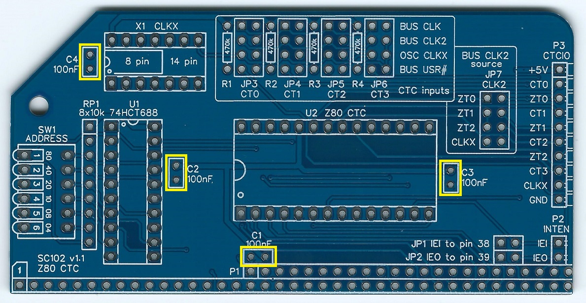
Fit and solder the 8x10k resistor network.

This must be fitted the correct way round. The component should have pin 1 marked with a dot, as illustrated right.

Bus Connector
Fit and solder bus connector P1.
You can fit just a single row header as used by the RC2014 Standard bus, but doing so means not all the features of this module can be used. It is best to fit a double row header even if the module is initially only used with a Standard bus backplane.
To prepare the header, it should first be cut to length (if starting with a strip more than 39 pins long) and then unwanted pins must be removed. If you want to make the board as easy to insert and remove as possible, you can remove all the pins in the second row except those shown on the schematic as used and indicated below in green.

Take care to ensure the pins are parallel to the circuit board so that the board will be vertical when plugged into a backplane.

Header Pins
Fit and solder the right-angled male header pins, P2 and P3.
Take care to ensure the pins are parallel to the circuit board.
Jumper Pins
Fit and solder the jumper pins for JP1 and JP2.
JP1 and JP2 are combined as a single, 2 row by 2 pin header.

Fit and solder the jumper pins for JP3 to JP7.
Each of these is a single, 2 row by 4 pin header.

Address Select Switch
Fit and solder the 6-way DIP switch SW1.
Take care not to overheat this component when soldering.
Inspection
Remove any solder ‘splats’ with a brush, such as an old toothbrush.
Visually inspect the soldering for dry joints and shorts.
Clean the flux off with suitable cleaning materials.
Visually inspect again.
Before fitting the ICs, plug the board into an RC2014 backplane with no other boards fitted. Power the backplane and perform the following checks with a voltmeter:
- Check the supply voltage on the CTC module, between, say, U1 pin 10 and U1 pin 20. This should be 4.5 to 5.5 volts, preferably 4.75 to 5.25 volts.
- Check each input (CT0, CT1, CT2, and CT3) on connector P3 is being pulled up to at least 4.5 volts.
- Check the interrupt enable input (IEI) on connector P2 is being pulled up to at least 4.5 volts.
- Check each address switch input (Q2 to Q7) on U1 is being pulled up to at least 4.5 volts when the appropriate switch (SW1) is Off (open) and drops to less than 0.4 volts when the appropriate switch (SW1) is On (closed).
- If you have an oscilloscope or logic probe, check the clocks CLK, CLK2 and CLKX (if oscillator X1 is fitted) at jumper header JP6.
If all is well, power down and remove the CTC module.
Integrated Circuits
Insert the ICs into their sockets, taking care to insert them the correct way round, as illustrated below. Be careful not to bend any legs over.

If the oscillator has not been soldered directly to the board, insert it into the socket now. The oscillator can be either the 8-pin or the 14-pin package size. The correct position for each is shown on the circuit board. In the case of the smaller 8-pin package, it is fitted right at the top end of the socket, as indicated by the notch on the socket. Pin 1 of the oscillator is normally indicated by a ‘sharp’ corner, while the other three corners are rounded.

Test
There is no need to fit any of the jumper shunts yet.
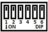
Set the DIP switches as shown below. This sets the address to the range 0x88 to 0x8B.
WARNING: The suggested addresses clash with the official RC2014 serial / ACIA module, which does not have tight address decoding. It is assumed that most people wanting a Z80 CTC module will be using a Z80 SIO as the serial device, as the ACIA can not generate Z80 mode 2 interrupts.
Now plug the CTC module into the RC2014 backplane together with your normal working set of modules. Power up and check the system is working as usual.
Circuit Explained
This RC2014 compatible module contains a Z80 CTC (counter timer channels) chip and is designed to be very flexible, with full access to the CTC’s hardware functions via header pins.
Address Decoding
The CTC is an I/O devices occupying a block of 4 I/O addresses. The base address of this block is set with DIP switches. These allow selection of any I/O address on a 4 byte boundary.
C1 to C4
These capacitors provide power supply decoupling (or bypass). The fast switching in digital circuits creates spikes on the power supply lines which are suppressed with decoupling capacitors placed at key points on the circuit board.
JP1 and JP2
This pair of jumpers allow the interrupt daisy chain signals to be connected to the RC2014 bus signal USER 2 (pin 38) and USER 3 (pin 39). To make use of this feature you must use a backplane that is specifically designed to provide the necessary daisy chain, such as Backplane SC107. The current official RC2014 backplanes do not support this feature.
Alternatively the signals IEI and IEO can be found on connector P2 on the back edge of the board. Dupont wires can be used to daisy chain these signals to other modules.
JP3 to JP6
JP3 to JP6 allow the source for each CTC input to be set to any of:
- RC2014 bus primary clock (CLK)
- RC2014 bus secondary clock (CLK2)
- This module’s on-board oscillator clock signal (CLKX)
- RC2014 bus USER pin (USER 4, 5, 6, 1 for CTC inputs 0, 1, 2, 3)
Without a jumper shunt fitted the input is from a pin on connector P3 on the back edge of the board.
JP7
JP7 allows the module to supply a clock signal to the RC2014 bus secondary clock (CLK2). The possible signal sources are:
- CTC channel 0 output (ZT0)
- CTC channel 1 output (ZT1)
- CTC channel 2 output (ZT2)
- This module’s on-board oscillator clock signal (CLKX)
P1
This connector mates with the RC2014 bus backplane. You can fit a single or a double row header, but the full functionality of this module requires the extended RC2014 bus and thus a double row header.
P2
As the official RC2014 backplanes do not provide a Z80 mode 2 interrupt daisy chain (IEI and IEO signals), these have been brought to the back of the board where they can be easily linked to other modules with Dupont wires.
P3
This connector brings power, oscillator output, CTC inputs and CTC outputs, to the back of the PCB. This makes it easy to connect via Dupont wires to other cards or to breadboards.
This connector also allows a simple jumper shunt to connect the output of one CTC channel to the input of the next, thus allowing channels to be cascaded for greater range.
R1 to R4
These resistors provide pull-ups for the CTC inputs so that they do not float up and down in the event a jumper is left off.
Version 1.0 of the schematic and PCB label these as 100k, but it was found that if all four inputs were set to the RC2014 bus primary clock (CLK) the system would become unreliable. The value has therefore changed to 470k to reduce loading of the clock signal.
RP1
This is a network of 8 resistors with one end of each resistor common to pin 1. The resistors are used to pull up the address select switch (SW1) outputs and also to pull up the interrupt enable input signal (IEI).
SW1
This switch is used to set the I/O address for the module. It sets the required state of address lines A2 to A7, thus allowing the module to occupy a 4 address block on any 4-byte boundary.
In order to provide some certainty for software it is strongly recommended you set the base address of your first CTC module to 0x88, so that the module occupies I/O addresses 0x88 to 0x8B. This is done by setting switches 1 to 6, to Off, On, On, On, Off, On, where On is the switch closed. In the case of the piano style DIP switch, the On position is the switch lever pushed down towards the circuit board.
Switches in the On position pull down the input of the address comparator U1. Switches in the Off position allow the input of the address comparator to be pulled up by RP1.
U1
This integrated circuit provides the address decoding, by comparing the current I/O address from the CPU with the address set with the DIP switch SW1.
U2
The Z80 CTC provides a four channel programmable counter/timer.
All four channels have an external clock/trigger input, and the first three channels have a zero count/time-out output. All of these signals are available on connector P3 on the back edge of the board.
Each counter/timer channel can be started as a timer by an external trigger signal on the channel’s input.
Each counter/timer channel can count down from a pre-set value, each time the selected edge (rising or falling) occurs on its input. When the counter reaches zero the counter is automatically reloaded and an optional interrupt generated.
Feeding a clock signal to a CTC channel input enables the CTC to generate a periodic tick signal and/or interrupt. Jumper options allow each channel to be optionally supplied with a clock signal from one of these sources:
- RC2014 bus primary clock (CLK)
- RC2014 bus secondary clock (CLK2)
- The CTC’s on-board oscillator output (CLKX)
- RC2014 bus USER pin (USER 5, 6, 7, 1 for CTC channels 0 to 3)
- An external signal from connector P3
The first three channels can each act as a baud rate generator by generating a periodic output at the required frequency, as described in the User Guide.
By pre-setting a channel’s counter to 1 the CTC can generate a Z80 mode 2 interrupt each time the selected edge occurs on the channel’s input. This allows the CTC to act as a four channel Z80 mode 2 interrupt controller for non-Z80 devices.
For further details see the Zilog CTC data sheet.
X1
This oscillator is optional. If fitted it can perform a number of functions:
- Source for the RC2014 primary bus clock (CLK)
- Source for the RC2014 secondary bus clock (CLK2)
- Source for any or all of the CTC clock inputs
The assumption is that a 7.3728 MHz oscillator is used. By using this value the board will match the frequency expected by software designed for this board. It will also enable the oscillator to be useful as a source for the RC2014 bus clocks CLK and CLK2, which are usually 7.3728 MHz.
If this oscillator is not fitted, the board can be configured with jumpers to use either of the RC2014 bus clocks as a source for any or all of the CTC inputs.
Fault Finding
First do the following:
- Carefully inspect all soldering.
- Check all the components are in the right place.
- Check all ICs for bent legs which are not making contact with their socket.
- Check all ICs are inserted the right way round.
Simple Voltage Tests
Remove all jumper shunts from the CTC module. Plug the CTC module in to the RC2014 compatible backplane with no other modules fitted. Power the backplane and perform the following checks with a volt meter:
- Check the supply voltage on the CTC module, between, say, U1 pin 10 and U1 pin 20. This should be 4.5 to 5.5 volts, preferably 4.75 to 5.25 volts.
- Check each input (CT0, CT1, CT2 and CT3) on connector P3 is being pulled up to at least 4.5 volts. The pull-up resistors are 470k so if your measuring device is not high impedance you will likely not see as much as 4.5 volts due to loading.
- Check the outputs (ZT0, ZT2 and ZT2) on connector P3. These should each be a low digital level, less than 0.5 volts.
- Check the interrupt enable input (IEI) on connector P2 is being pulled up to at least 4.5 volts.
Input Clock Signals
With the set up the same as above, do the following:
Check the clock signals CLK and CLKX at jumper header JP6. The set of pins nearest the on-board oscillator are the ones carrying these signals.
If you only have a meter, the voltage should be around 2.5 volts. If it is outside the range of 2 to 3 volts you may have a problem with the clock signal.
If you have a logic probe it should indicate the signal is oscillating.
If you have an oscilloscope you should see sensible digital clock signals on these pins. The frequencies should match the bus clock and the on-board clock oscillator.
Basic Operation
Set the address selection switches shown below (base address 0x88, giving a range of 0x88 to 0x8B).

Fit a single jumper shunt as indicated below (in yellow). CTC channel 1 should now be clocked from the primary bus clock (CLK).

Install a working set of RC2014 compatible modules into the backplane, together with the CTC module.
From the Small Computer Monitor, enter the following commands to set CTC channel 1 to generate a 0.6144 MHz clock on its output (assuming the bus clock is 7.3728 MHz) .
- O 89 55
- O 89 6
If all you have in the way of test equipment is a meter, then measure the output voltage of channel 1 (signal ZT1 on header P3). You should see a significant change when the above commands have been entered. A measurement here with a digital multi-meter showed a change from 0 volts to 0.5 volts.
A logic probe could be used to check the output of channel 1 (signal ZT1 on header P3) changes from a steady state to oscillating.
If you have an oscilloscope, verify he output of channel 1 (signal ZT1 on header P3) is 0.6144 MHz (assuming the bus clock is 7.3728 MHz).
If there is no output, check the input clock to channel 1 (signal CT1 on header P3).
If you are unable to verify the CTC output using test equipment, then check channel 1’s counter is functioning by repeatedly reading the counter’s value using Small Computer Monitor’s Input command (I, not 1):
- I 89
As the counter should be changing fast, the value displayed by reading the counter should be random, in the range of 0 to 6. If the same value is displayed each time, then the CTC is not counting (or you are beating the odds of ‘random’).
Address Decoding
If the above tests show there is a problem, then check the address decoding:
Check the output of the address comparator U1, pin 19, is a logic high level of at least 4 volts.
Enter the following code with the Small Computer Monitor’s Assemble command (A):
- a 8000
- in a,(89)
- jp 8000
Exit assemble mode with the Escape key and then run the program with the Go command (G):
- g 8000
This program continually reads from the CTC, so you should see activity on the address comparator’s output. With a simple meter this will show as a voltage drop. In my case from 4.9 volts when the code is not running to 4.3 volts when it is running.
If the address decoding does not seem to be functioning as described above, do the following:
- Check each address switch input (Q2 to Q7) on U1 is being pulled up to at least 4.5 volts when the appropriate switch (SW1) is Off (open) and drops to less than 0.4 volts when the appropriate switch (SW1) is On (closed).
- Check there is activity on the comparator’s address bus inputs (P2 to P7).
- Check the comparator’s inputs P0, P1, Q0 and Q1 are all logic low, of less than 0.5 volts.
If all the above checks look good, but the comparator’s output does not appear correct, then it is likely the comparator chip (U1) is faulty or there is a short on the output signal.
Interrupts
None of the above tests use interrupts, so the system’s /INT signal should remain high.
Notes
- This design is made in accordance with the “designed for RC2014” labelling scheme.
- RC2014 is a trademark of RFC2795 Ltd.
- This product is designed for hobby use and is not suitable for industrial, commercial or safety-critical applications.
- The product contains small parts and is not suitable for young children.
