Someone recently asked me a few questions about design, which got me thinking about writing a series of posts for this website.
I hope to encourage anyone who has considered designing their own retro computer add-on, or indeed a whole system, to have a go. Getting that first professional looking PCB in the post is very rewarding and is relatively cheap.
Don’t overthink it
Don’t be put off because you don’t know the characteristics of different logic chip families, or how to work out the correct value of a resistor, or any of the other issues. Don’t overthink it. I’m not suggesting that these things aren’t important, just that they are not as critical as you might expect.
Most of the time you don’t need to work out all the signal timings or any of the other complex stuff. Often the components have been designed to work together and you just don’t need to worry about them.
I dare say some of you serious designers will point out the error of this simplistic approach, but it works pretty well for me.
In this first post I’ll describe the process of designing a very simple circuit board.
First decide what you are going to build
This may sound obvious but failure to properly decide what you are trying to achieve is actually an easy mistake to make.
Don’t just think about it, write it down. If you can’t write a short concise description of your goal then I’d strongly suggest you are not ready for the next step.
In this post we will follow the example of a simple project to light an LED when a button is pressed. This would be my project description:
An example project which simply lights an LED when a push button switch is pressed.
Specification
Next, we need to write a more detailed specification. It might be something like this.
The project will be constructed entirely on a small printed circuit board.
The circuit board will house a screw terminal to connect the 5 volt power supply, a small tactile push button switch, and a green LED. A resistor will also be required to limit the LED current.
The only function of the board is to light the LED when the button is pressed.
We now have a pretty good idea of what the project is going to involve.
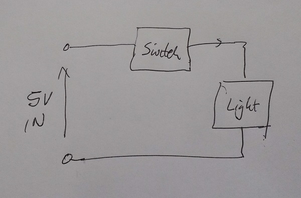
Block diagram
Next, sketch a block diagram of the electronics.
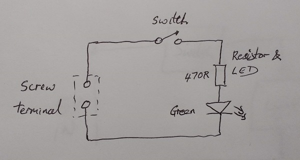
Circuit diagram
It is probably also worth sketching out a circuit diagram. A quick sketch could save lots of time when you go to draw a professional looking schematic on the computer.
Design software
These days the bulk of the design work is done on a computer.
You could now use a computer to ‘draw’ a picture of the tracks and holes on the circuit board and send the design off to be turned into a printed circuit board. However, it is far better to use a software package which links a schematic to a circuit board design. Once you have a schematic the software can help you lay out the circuit board.
In this example, we will use EasyEDA software. This is a free web based program which does not require installation on your computer. In case you were wondering, “EDA” stands for Electronic Design Automation.
EasyEDA
Use your browser to go to EasyEDA.com and create an account.
EasyEDA is constantly improving their software so what follows may become dated over time. Also, this is only a very brief tutorial. You will need to experiment to discover the vast majority of the software’s features.
In the EasyEDA editor, select a New Project from the file menu.

The New Project dialog will ask for a project Title.
You should now be presented with a blank schematic, something like this:
We now need to draw our schematic (or circuit diagram). This involves selecting components from the library and placing them on the schematic.
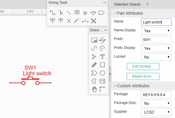
Some of the common components can be found in the EELib, as illustrated below. Scroll to the required component, click on it and then click on the schematic.

Once placed on the schematic, components can be dragged into the required position and rotated. Components can be named as illustrated below.
If you can’t find the component you require in the EELib, click on Libraries and locate it as shown below.

To connect the components, either drag them until they touch, as shown with the switch, resistor and LED below, or use the WIRE tool.

The illustration below shows the circuit complete, except I’ve failed to connect the screw terminal to the switch. The design manager indicates the components that have not been connected. You will need to click on the refresh icon next to the Net List to get it to update.
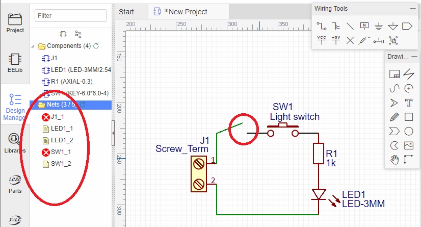
The design manager is important as it shows the Net List. The Net List is used when laying out the circuit board to check all the connections match those on the schematic. This saves a lot of time and worry, so make sure your schematic is correct and no errors are reported in the Net List.
Once the schematic is complete, save it and then select Convert to PCB.

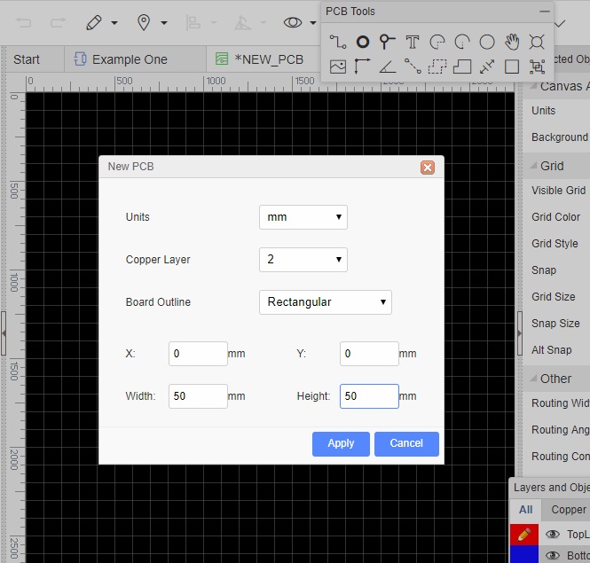
Fill in the New PCB dialog, as shown below.
The PCB is displayed, as shown below. Initially, the components are not in any sensible positions.
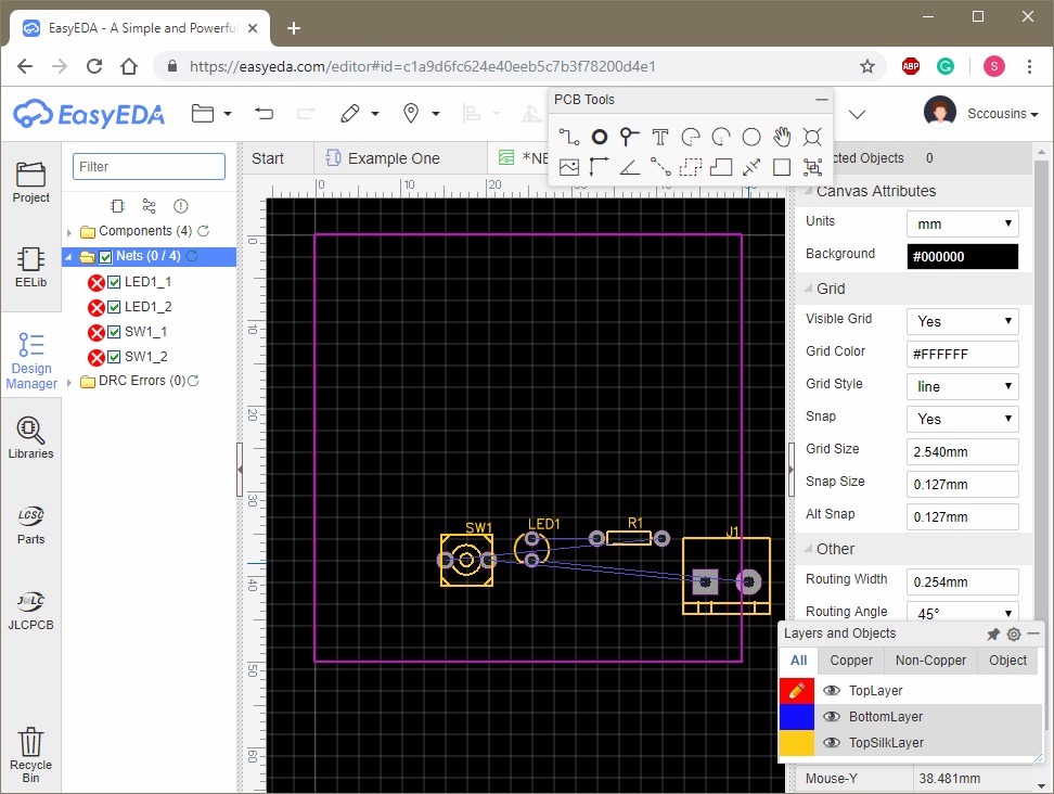
Drag the components to the required positions. Notice the “Ratlines” between the component terminals. These are the connections required to match the Net List, described earlier. Also, notice the errors in the Net List on the left.
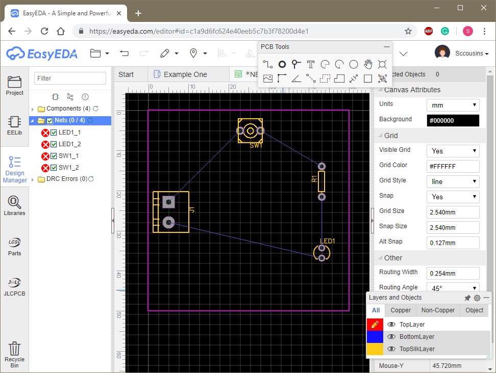
Use the TRACK tool to run tracks between the components. When each connection is made the associated Ratline disappears. Click on the refresh icon in the Net List to check the connections have all been made.

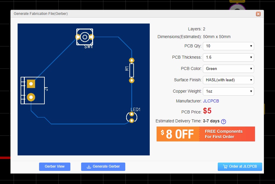
Save the PCB design and select “Generate Fabrication File” (in the file menu). You will be asked if you would like to “Check DRC”. The Design Rule Check (DRC) will warn you if tracks and holes are too close, so always use it before getting a board made.
If you select “No, Generate Gerber”, you should be presented with a picture of your design and a quote for fabrication at JLCPCB.
In part 2 of this series we start taking a more detailed look at the design process.
