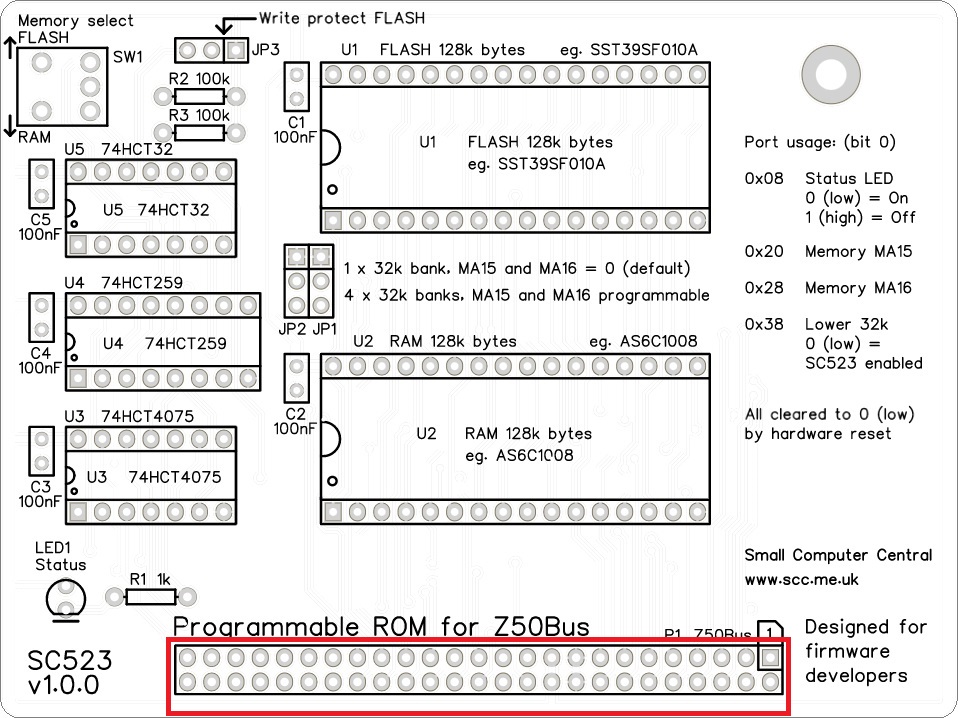
SC523 is a Z80 programmable ‘ROM’ card for firmware developers, designed for Z50Bus.
Documentation
- SC500 – Series Information
- SC523 – Description
- SC523 – Assembly Guide
- SC523 – Firmware, SCM F2
- SC523 – Parts List
- SC523 – Printed Circuit Board
- SC523 – Software, CP/M 2.2
- SC523 – Software, SCM Apps
- SC523 – Support
- SC523 – User Guide
Downloads
Kits
Description
SC523 is a Z80 programmable ‘ROM’ card designed for Z50Bus.

This card is designed for firmware developers.
It provides the read-only memory for a Z80-based system. In this case, however, the term “read-only” is not really correct as data can be written to it.
The card houses a FLASH chip which contains the boot-up firmware, such as the Small Computer Monitor (SCM). It also houses a “shadow” RAM chip (pseudo-ROM) which is arranged such that writing to the ‘ROM’ area causes the data to be written to the “shadow” RAM.
Once the “shadow” RAM contains the required firmware image, the memory select switch can be used to reconfigure the memory such that reading is from “shadow” RAM, which is now write-protected.
The main features are:
- 128k bytes FLASH (4 banks of 32k bytes)
- 128k bytes RAM (shadow ‘ROM’)
- Status LED
- Jumper selection of memory bank, or
- Software control of memory bank
- Write protect jumper for FLASH memory
- Compatible with Z80 CPU card SC518 plus memory card SC519
- Compatible with Z80 processor SC516
- The card can be disabled by writing to port 0x38
A typical system will also requires:
- Backplane (eg. SC501, SC508, SC515, or SC522)
- Power and reset card (eg. SC502)
- Z80 CPU and memory:
- Z80 processor card (eg. SC516 with ROM chip removed), or
- Z80 CPU + Z80 memory (eg. SC518+SC519 with FLASH chip removed)
- Serial card (eg. SC511, SC520, or SC521)
User Guide
SC523 is a Z80-compatible programmable ‘ROM’ card designed for Z50Bus.

This card is designed for firmware developers. It provides the read-only memory for a Z80-based system. In this case, however, the term “read-only” is not really correct as data can be written to it.
The card contains “shadow” RAM which is arranged such that writing to the ‘ROM’ area causes the data to be written to the “shadow” RAM. Once the “shadow” RAM contains the required ROM image, the memory select switch can be used to reconfigure the memory such that reading is from “shadow” RAM, which is now write-protected.
A minimal system using this card also requires:
- Backplane (eg. SC501, SC508, SC515, or SC522)
- Power and reset card (eg. SC502)
- Z80 CPU and memory:
- Z80 processor card (eg. SC516 with ROM chip removed), or
- Z80 CPU + Z80 memory (eg. SC518+SC519 with FLASH chip removed)
- Serial card (eg. SC511, SC520, or SC521)
The standard ROM (or Flash) memory chip needs to be removed from its normal card (eg. SC516 or SC519). This allows SC523 to provide the ‘ROM’ without conflict.
SC523’s Flash memory socket (U1) should contain suitable firmware. Typically this is SCM F1 or SCM F2. SCM F1 supports SC516’s serial port but does not support SC523’s software-controlled memory bank selection. SCM F2 does not support SC516’s serial port but does support SC523’s software-controlled memory bank selection. Firmware developers are likely to want a good serial port, not the very basic port on SC516, thus SCM F2 is likely to be the most appropriate configuration.
The firmware development process
This card replaces the Flash/ROM chip in a Z80 system.
The SC523 card houses a Flash/ROM chip containing standard firmware (eg. SCM F2) and also a “shadow” RAM chip (pseudo-ROM).
Starting with a functioning Z80 system, remove the Flash/ROM chip. Insert SC523 into the backplane and set its switch to the “FLASH” position.
The system is booted up from the standard Flash/ROM chip in SC523, which is assumed to contain the Small Computer Monitor (SCM) configuration F2.
Any writes to the lower 32k of memory are directed to the “shadow” RAM chip on SC523.
Trial firmware code is written to the “shadow” RAM, typically by sending a hex file of the firmware to be tested via the Small Computer Monitor (SCM). This process is detailed here.
The function of the Flash/ROM and “shadow” RAM is then swapped with the toggle switch to allow the trial firmware to be tested without having to program a Flash/ROM chip.
It is advisable to press and hold the reset button while swapping the chip functions to prevent memory corruption during the change-over.
Minor tweaks to the trial firmware can be made using SCM as memory writes are directed to the “shadow” RAM chip. However, this can be confusing as SCM will always read the existing memory contents from the SCM ROM and not from the “shadow” RAM.
The whole card can be paged out of memory with the usual write to port address 0x38.
Below is an example:
- With SC523 present but the Flash/ROM chip removed from the pre-existing system, turn on. The firmware in the Flash/ROM of SC523 will then run. This is assumed to be the Small Computer Monitor, configuration F2.
- Build whatever firmware you want to test using your favourite tools. The result needs to be an Intel HEX file with code starting at address 0x0000.
- Use a terminal program, such as Tera Term to “send” the HEX file to SCM. This essentially pastes the HEX file into the terminal window as if it had been typed very quickly.
- SCM should respond with “Ready” if the file is received correctly. As the file is received it is written to the shadow RAM on SC523.
- Press and hold the reset button, then toggle the switch on SC523 from the “FLASH” position to the “RAM” position. Release the reset button.
- Your firmware in shadow RAM is now paged into the Z80 memory map starting at address 0x0000 and is write protected. When the reset button is released your firmware is executed as if it were programmed into a Flash/ROM chip.
- Minor modifications can be made by switching back to the Flash/ROM and using SCM to edit memory. Note that SCM cannot read from the pseudo RAM so you can’t see what is there when editing the memory. This can be rather confusing.
Using the above steps to test a modified version of SCM, this is the monitor output:
Booting from the Flash/ROM on SC523
Small Computer Monitor - Z50Bus/Z80
*?
Small Computer Monitor by Stephen C Cousins (www.scc.me.uk)
Configuration F2 20220227, Monitor 1.3.0, SCZ80 BIOS 1.3.0

Monitor commands:
A [<address>]  = Assemble        |  D [<address>...
M [<address>]  = Memory display  |  E [<address>...
R [<name>]     = Registers/edit  |  F [<name>]  ...
B [<address>]  = Breakpoint      |  S [<address>...
I <port>       = Input from port |  O <port> <da...
G [<address>]  = Go to program
BAUD <device> <rate>             |  CONSOLE <dev...
FILL <start> <end> <byte>        |  API <functio...
DEVICES, DIR, HELP, RESET
BASIC    Grant Searle's adaptation of Microsoft ...
WBASIC   Warm start BASIC (retains BASIC program)
CPM      Load CP/M from Compact Flash (requires ...
*
Sending the modified version of SCM as a HEX file
*Ready

*
*
Toggle to the modified version of SCM now in pseudo ROM
Note the version number is different from the SCM firmware in FLash/ROM
Small Computer Monitor - Z50Bus/Z80
*?
Small Computer Monitor by Stephen C Cousins (www.scc.me.uk)
Configuration F2 20221016, Monitor 1.3.1, SCZ80 BIOS 1.3.1

Monitor commands:
A [<address>]  = Assemble        |  D [<address>...
M [<address>]  = Memory display  |  E [<address>...
R [<name>]     = Registers/edit  |  F [<name>]  ...
B [<address>]  = Breakpoint      |  S [<address>...
I <port>       = Input from port |  O <port> <da...
G [<address>]  = Go to program
BAUD <device> <rate>             |  CONSOLE <dev...
FILL <start> <end> <byte>        |  API <functio...
DEVICES, DIR, HELP, RESET
BASIC    Grant Searle's adaptation of Microsoft ...
WBASIC   Warm start BASIC (retains BASIC program)
CPM      Load CP/M from Compact Flash (requires ...
*
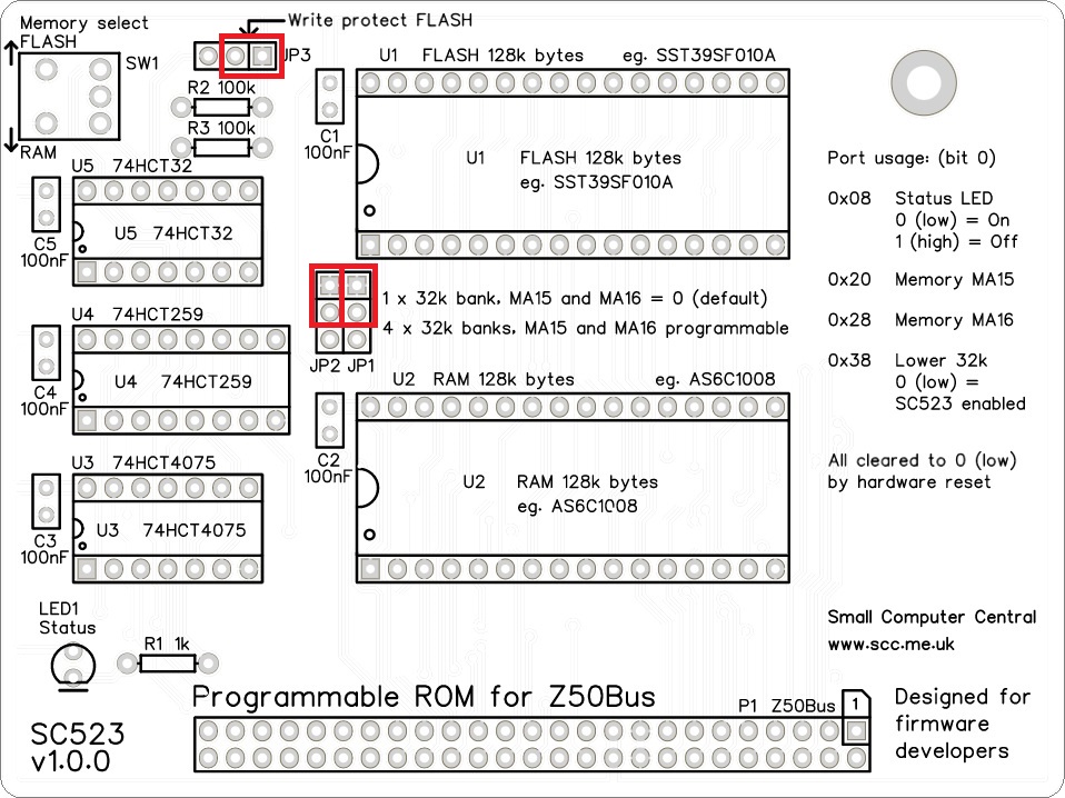
Default jumper settings
The illustration below shows the default jumper shunt positions. JP1 and JP2 select the bottom 32k bytes of the memory chips. JP3 write protects the Flash memory.
Memory map
This memory card is designed for use with a Z80 CPU.
Following a hardware reset, with the jumper shunts in their default positions and the toggle switch set to FLASH, the memory is mapped as indicated below. The upper 32k bytes of RAM are supplied by a separate card (eg. SC516 or SC519).
| Z80 memory range | Function/mapping |
| Lower 32k bytes 0x0000 to 0x7FFF | Read: SC523’s FLASH (U1) 0x00000 to 0x07FFF Write: “shadow” RAM (U2) 0x00000 to 0x07FFF |
| Upper 32k bytes 0x8000 to 0xFFFF | External RAM, read and write 0x08000 to 0x0FFFF eg. from SC516 or SC519 |
| SC523’s FLASH (U1) not visible to Z80 | 0x08000 to 0x1FFFF |
| SC523’s “shadow” RAM (U2) not visible to Z80 | 0x08000 to 0x1FFFF |
As above but the toggle switch set to RAM, the memory map
| Z80 memory range | Function/mapping |
| Lower 32k bytes 0x0000 to 0x7FFF | Read: “shadow” RAM (U2) 0x00000 to 0x07FFF Write: SC523’s FLASH (U1) 0x00000 to 0x07FFF |
| Upper 32k bytes 0x8000 to 0xFFFF | External RAM, read and write 0x08000 to 0x0FFFF eg. from SC516 or SC519 |
| SC523’s FLASH (U1) not visible to Z80 | 0x08000 to 0x1FFFF |
| SC523’s “shadow” RAM (U2) not visible to Z80 | 0x08000 to 0x1FFFF |
Writing to Flash memory requires JP3 to be set to enable writes and also the correct sequence of addresses must be issued to unlock the Flash chip for writing.
The memory map can be changed to all 64k being RAM, as needed for CP/M, by writing a 1 (high) to port 0x38 bit 0. The memory map is illustrated below. The 64k of RAM is supplied by an external card, such as SC516 or SC519. SC523 is completely disabled.
| Z80 memory range | Function/mapping |
| Lower 32k bytes 0x0000 to 0x7FFF | External RAM, read and write 0x00000 to 0x07FFF |
| Upper 32k bytes 0x8000 to 0xFFFF | External RAM, read and write 0x08000 to 0x0FFFF |
| SC523’s FLASH (U1) not visible to Z80 | 0x00000 to 0x1FFFF |
| SC523’s “shadow” RAM (U2) not visible to Z80 | 0x00000 to 0x1FFFF |
Jumper options
With the jumper shunts in the default positions, the FLASH memory (U1) is protected against being written to and the first 32k bank of the Flash (U1, read) and RAM (U2, write) is mapped into the Z80’s memory from 0x0000 to 0x7FFF.
JP1 shunt can be moved to the “Write enable” position if you want to update the firmware in FLASH memory (U1). This requires appropriate software which is not currently available (as far as I know). The shunt can be left in this position as it is very unlikely the FLASH memory will be written to without special software. The IC requires a very specific sequence in order to accept write operations. For peace of mind, it is best to fit the shunt in the “Write protect” during normal use.
JP2 and JP3 allow one of four 32k banks of the FLASH (U1) and RAM (U2) to be selected. This allows easy selection of up to four different firmware programs. Alternatively, bank selection can be set for software control. Software control allows the four banks to be manipulated by two output port bits. This enables software to access all 128k of the FLASH (U1) and RAM (U2).
Status LED
When using the Small Computer Monitor ‘ROM’, pressing the reset button should cause the status LED to flash.
- One flash off and on indicates a serial card has been detected on the bus and is being used to connect to a terminal. Serial cards usually work at 115200 baud, 8 data bits, 1 stop bit, no parity, and hardware flow control (RTS/CTS).
- Continuous flashing means the RAM test has failed.
After this, the LED is available for use by any software. Just write to port 0x08 (or decimal 8) to control the LED. See table below.
Output port bits
This card uses the following output port and bits.
| Port | Bit | Function |
| 0x08 | 0 | Status LED 0 (low) = ON 1 (high) = OFF |
| 0x20 | 0 | Memory bank select (MA15) |
| 0x28 | 0 | Memory bank select (MA16) |
| 0x38 | 0 | Lower 32k select 0 (low) = Enabled SC523 1 (high) = Disabled SC523 |
| Upper 32k is always RAM |
All of the above bits are cleared to 0 (low) by a hardware reset.
Parts List
| Reference | Qty | Component |
| PCB | 1 | SC523, v1.0, PCB |
| C1 to C5 | 5 | Capacitor, ceramic, 100 nF |
| JP1 to JP3 | 3 | Header, male, 1 x 3 pin, straight |
| Jumper shunts | 5 | Jumper shunt Two used to pad box header |
| LED1 | 1 | LED, green, 3mm, angled |
| P1 | 1 | Box header, 2 x 25 pin, angled, or Header, male, 2 x 25 pin, angled |
| R1 | 1 | Resistor, 1k, 0.25W |
| R2 and R3 | 2 | Resistor, 100k, 0.25W |
| SW1 | 1 | Switch, toggle, sub-miniature, SPDT |
| Spacer | 1 | Spacer, 10mm, M3, nylon |
| Screw (for spacer) | 1 | Machine screw, 6mm, M3 |
| U1 | 1 | Flash 128k bytes SST39SF010A (typically containing SCM F2) |
| U1 socket | 1 | 32-pin DIP socket |
| U2 | 1 | RAM 128k bytes AS6C1008 |
| U2 socket | 1 | 32-pin DIP socket |
| U3 | 1 | 74HCT4075 |
| U3 socket | 1 | 14-pin DIP socket |
| U4 | 1 | 74HCT259 |
| U4 socket | 1 | 16-pin DIP socket |
| U5 | 1 | 74HCT32 |
| U5 socket | 1 | 14-pin DIP socket |
Printed Circuit Board
| Supplier | Website | Ships from |
| Stephen C Cousins | Tindie | UK |
| pcb4diy | pcb4diy.de | Germany |
| pcb4diy | eBay | Germany |

Assembly Guide
Important note: How to modify box headers
There shouldn’t be any surprises to catch you out, so experienced builders can just go ahead and populate the board.
This guide assumes you are familiar with assembling circuit boards, soldering, and cleaning. If not, it is recommended you read some of the guides on the internet before continuing.
First check you have all the required components, as listed in the parts list.
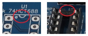
Before assembling it is worth visually inspecting the circuit board for anything that looks out of place, such as mechanical damage or apparent manufacturing defects.
If you have a multimeter that measures resistance or has a continuity test function, check there is not a short on the power supply tracks. Connect the probes to each terminal of one of the capacitors, such as C1. This should be an open circuit, not a short circuit.
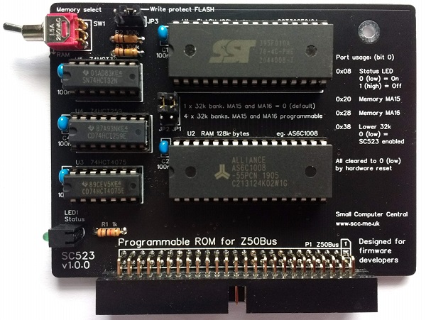
The picture below shows what a completed SC523, Z80 Programmable ‘ROM’ Card should look like.
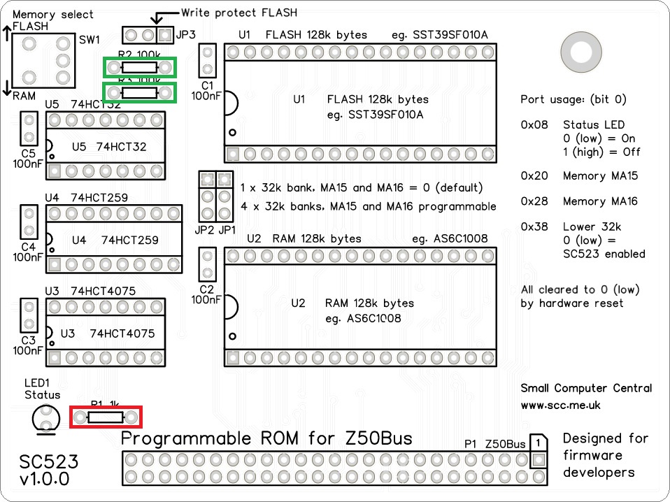
Resistor
Fit and solder the 1k resistor, R1 (shown below in red).

Fit and solder the two 100k resistors, R2 and R3 (shown below in green).

Resistors can be fitted either way around, as they are not polarity dependent.
IC sockets
Fit and solder IC sockets for U1 to U5.
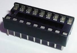
Be sure to fit them with the notch matching the legend on the circuit board, so you do not end up fitting the IC the wrong way around too.

Capacitors
Fit and solder capacitors C1 to C5.
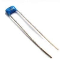
These can be fitted either way around, as they are not polarity dependent.

Light Emitting Diode (LED)
Fit and solder green LED, LED1.
If using an angled LED the polarity is predefined and matches the PCB.
If using a standard LED care must be taken to ensure it is fitted the correct way around.
It is important to fit the LED the correct way around. LEDs usually have a small flat side to indicate the cathode (the negative end). This should be positioned to match the flat side shown on the circuit board (illustrated to the right). Also, the cathode pin on the LED is usually shorter than the other pin (the Anode).


Jumper Header Pins
Fit and solder header pins JP1, JP2, and JP3.
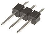
This header may need to be cut down from a longer strip.

Bus connector
Fit and solder the bus connector, P1. This can either be a right-angled box header or right-angled header pins. The box header is recommended.
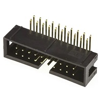
Take care to ensure the connector is fitted such that the card will stand vertically when fitted to a backplane. A good method is to just solder two pins, one at each end, and then check it looks correct. Then solder two more, one at each end but in the other row, and check again. At each stage, if necessary, adjust the position by heating the required solder joint and moving the connector slightly. Solder two pins in the middle of the connector and check again. Then solder all the others.
Inspection
Remove any solder ‘splats’ with a brush, such as an old toothbrush.
Visually inspect the soldering for dry joints and shorts.
Clean the flux off with suitable cleaning materials.
Visually inspect again.
Integrated Circuits
Insert the ICs into their sockets, taking care to insert them the right way around, as illustrated below. Be careful not to bend any legs over. ICs are usually supplied with the legs slightly spread out making them difficult to insert. It is best to bend the two rows of legs so they are parallel before inserting them. Remember, these components can be damaged by static electricity so if possible earth yourself and the components while handling them.

SC523’s Flash memory socket (U1) should contain suitable firmware. Typically this is SCM S2 or SCM S3. SCM S2 supports SC516’s serial port but does not support SC523’s software-controlled memory bank selection. SCM S3 does not support SC516’s serial port but does support SC523’s software-controlled memory bank selection.
Configuration
Fit jumper shunts in the positions shown below.
Fault Finding
Check there are no chips with bent legs and thus not making contact with their socket, carefully inspect all soldering, check all the chips are inserted the right way around, check all the components are in the right place.
Fit this card into a backplane together with a suitable set of cards to make a working system and then power up. A minimal system using this card also requires:
- Backplane (eg. SC501, SC508, SC515, or SC522)
- Power and reset card (eg. SC502)
- Z80 CPU and memory:
- Z80 processor card (eg. SC516 with ROM chip removed), or
- Z80 CPU + Z80 memory (eg. SC518+SC519 with ROM chip removed)
- Serial card (eg. SC511, SC520, or SC521)
Check the LED is on. If it is not, then check the LED is the correct way around. Also check the RESET signal is high but goes low when the reset button is pressed. The LED should light when U4 is powered and working, and the RESET signal on U4 pin 15 is low.
If the LED is working, check it flashes off and then on again following a reset. If it flashes then the board is running code successfully. This would indicate that all the main components are generally working. If it keeps flashing the self-test has failed, most likely indicating the RAM is not working.
Notes
- This design is made with the permission of LiNC (designers of the Z50Bus).
- This product is designed for hobby use and is not suitable for industrial, commercial, or safety-critical applications.
- The product contains small parts and is not suitable for young children.
