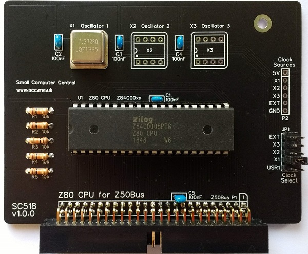
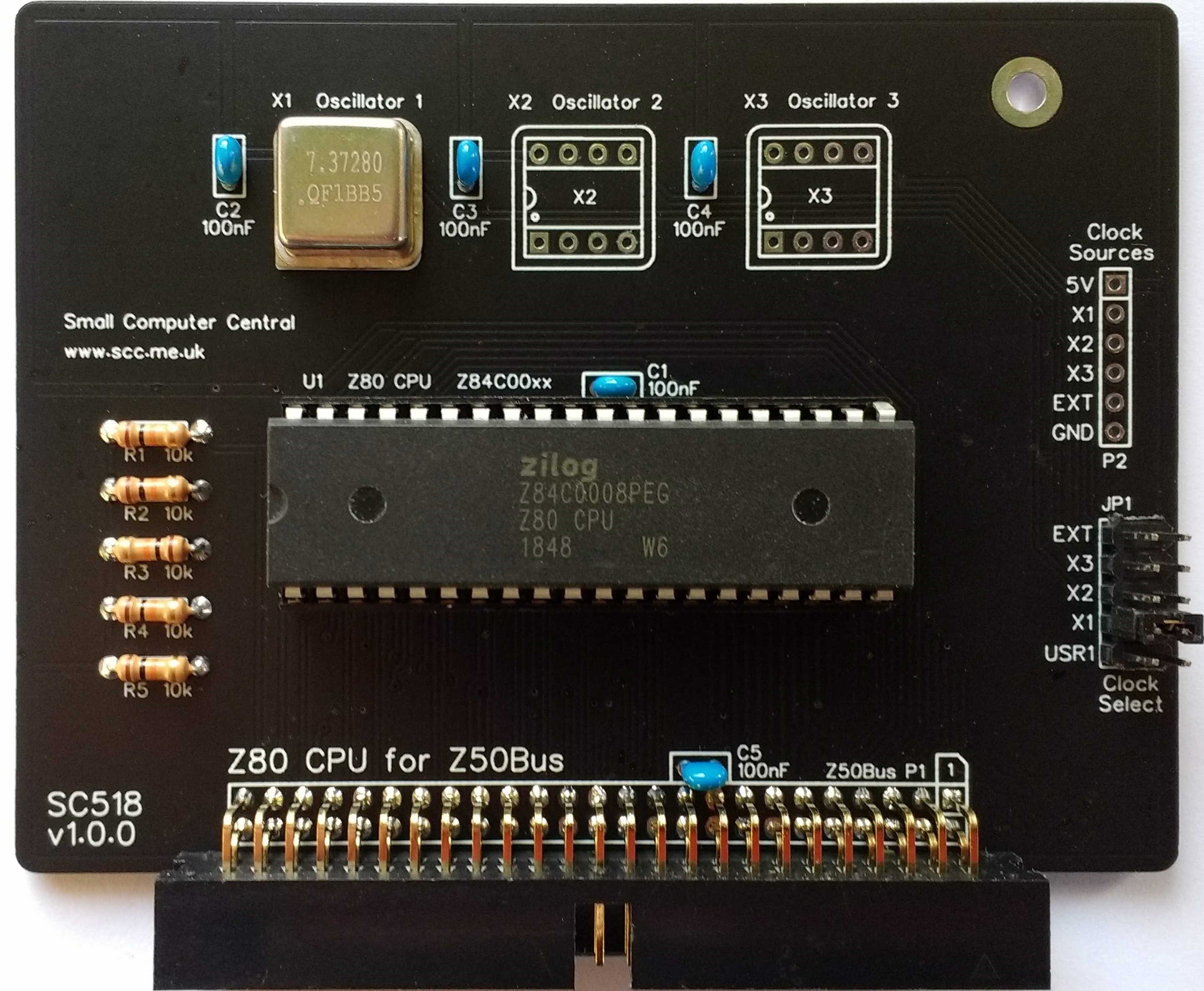
SC518 is a Z80 Central Processor Unit (CPU) card designed for Z50Bus.
Documentation
- SC500 – Series Information
- SC518 – Description
- SC518 – Assembly Guide
- SC518 – Firmware – see memory card (eg. SC519)
- SC518 – Parts List
- SC518 – Printed Circuit Board
- SC518 – Software, CP/M 2.2 (see SC519)
- SC518 – Software, SCM Apps
- SC518 – Support
- SC518 – User Guide
Downloads
Kits
Description
SC518 is a Z80 CPU card designed for Z50Bus.
This card provides a Z80 CPU with a choice of clock sources.
The main features are:
- Z80 Central Processor Unit (CPU)
- Jumper to select one of 5 clock sources:
- Half-size (8-pin DIP) “can” oscillator (x 3)
- Bus pin USR1
- External pin
- Typical clock speed 7.3728 MHz
- Compatible with memory card SC519
This card is designed to allow easy selection of a number of different clock sources for the Z80 CPU.
A typical system will also require:
- Backplane (eg. SC501)
- Power supply (eg. SC502)
- Memory card (eg. SC519)
- Serial card (eg. SC521)
Parts List
| Reference | Qty | Component |
| PCB | 1 | SC518, v1.0, PCB |
| C1 to C5 | 5 | Capacitor, ceramic, 100 nF |
| JP1 | 1 | Header, male, 2 x 5-pin, angled, or Header, male, 2 x 5-pin, straight |
| Jumper shunts | 3 | Jumper shunt Two used to pad box header |
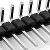
| P1 | 1 | Box header, 2 x 25 pin, angled, or Header, male, 2 x 25 pin, angled |
| P2 | 1 | Header, male, 1 x 6-pin, angled, or Header, male, 1 x 6-pin, straight |
| R1 to R5 | 5 | Resistor 10k 0.25W |
| Spacer | 1 | Spacer, 10mm, M3, nylon |
| Screw (for spacer) | 1 | Machine screw, 6mm, M3 |
| U1 | 1 | Z80 CPU Z84C0008PEG, or Z80 CPU Z84C0010PEG |
| U1 socket | 1 | 40-pin DIP socket |
| X1 | 1 | Oscillator 7.3728 MHz |
| X2 and X3 | 2 | Oscillator (optional) |
| X1 to X3 socket | 3 | 8-pin PDIP socket (optional) |
Printed Circuit Board
| Supplier | Website | Ships from |
| Stephen C Cousins | Tindie | UK |
| pcb4diy | pcb4diy.de | Germany |
| pcb4diy | eBay | Germany |
User Guide
SC518 is a Z80 CPU card designed for Z50Bus.
Card features:
- Z80 Central Processor Unit (CPU)
- Jumper to select one of 5 clock sources
- Typical clock speed 7.3728 MHz
- Compatible with memory card SC519
This card is designed to allow easy selection of a number of different clock sources for the Z80 CPU.
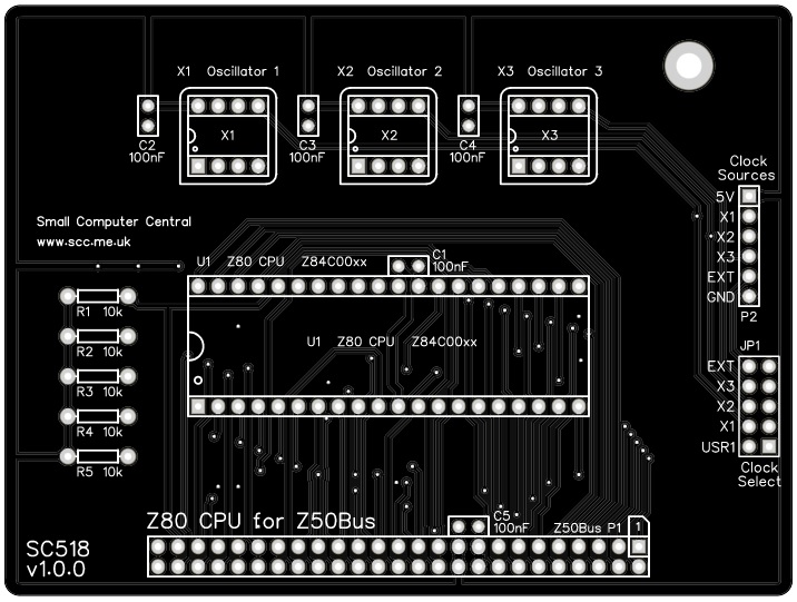
Clock source
The clock source is selected by fitting a jumper shunt to the required position on JP1. The available clock sources are:
- External pin (pin 5 of connector P2)
- Oscillator X1 (half-size 8-pin DIP ‘can’ oscillator)
- Oscillator X2 (half-size 8-pin DIP ‘can’ oscillator)
- Oscillator X3 (half-size 8-pin DIP ‘can’ oscillator)
- Bus pin USR1 (pin 39 of the Z50Bus)
Up to three oscillators can be fitted (X1 to X3). This allows three different clock speeds to be readily available.
Alternatively, the clock signal can be provided on the Z50Bus pin 39 (USR1) or an external signal pin on connector P2. These signals can be clock rates from D.C. (zero Hertz) to the maximum the Z50Bus can support (typically 8 MHz but with suitable components, it could be 20 MHz).
System requirements
In order to build a minimal working system you will also need:
- Backplane, eg:
- SC501 – 7-slot backplane
- SC508 – 10-slot backplane
- SC513 – 6-slot backplane plus 5-volt power input
- SC515 – 14-slot backplane
- SC522 – 6-slot backplane
- Power supply, eg:
- SC502 – Power supply card (8 to 15 volt input)
- SC513 – 6-slot backplane plus 5-volt power input
- Memory card, eg:
- SC519 – 128k Flash ‘ROM’ plus 128k RAM
- Serial card, eg:
- SC511 – Z80 SIO (2 ports) plus CTC (baud rates and timer)
- SC520 – ACIA 68B50 (1 port) plus baud rate generator
- SC521 – Z80 SIO (2 port) plus baud rate generators
Assembly Guide
Important note: How to modify box headers
Experienced builders
There is only one suggested build option to watch out for. You can fit either a straight or a right angled header to P2. Other than that there shouldn’t be any surprises to catch you out, so experienced builders can just go ahead and populate the board.
This guide assumes you are familiar with assembling circuit boards, soldering, and cleaning. If not, it is recommended you read some of the guides on the internet before continuing.
First check you have all the required components, as listed in the parts list.
Before assembling it is worth visually inspecting the circuit board for anything that looks out of place, such as mechanical damage or apparent manufacturing defects.
If you have a multimeter that measures resistance or has a continuity test function, check there is not a short on the power supply tracks. Connect the probes to each terminal of one of the capacitors, such as C1. This should be an open circuit, not a short circuit.
The picture below shows what a completed SC518, Z80 CPU Card should look like.
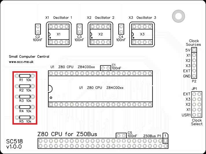
Resistors
Fit and solder the 10k resistors R1 to R5 (shown below in red).
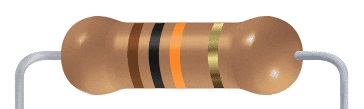
These can be fitted either way around, as they are not polarity dependent.
IC socket
Fit and solder IC socket for U1.
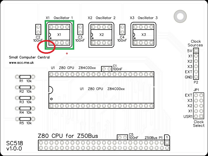
You may wish to fit a socket for oscillator X1. My preference is to solder this component, which you do later.
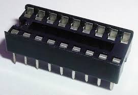
Be sure to fit the socket with the notch matching the legend on the circuit board, so you do not end up fitting the IC the wrong way around too.

Capacitors
Fit and solder capacitors C1 to C5.
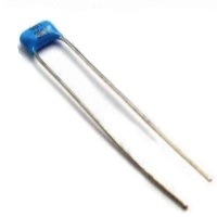
These can be fitted either way around, as they are not polarity dependent.

Jumper Header Pins
Fit and solder jumper header pins JP1.

This header may need to be cut down from a longer strip.
Clock Source Header
Fit and solder connector P2.
You can either fit straight pins or angled pins.
Angled pins give better access when mounted on a backplane, but straight pins are less obtrusive.
This header may need to be cut down from a longer strip.
Take care to ensure the pins are perpendicular (straight pin) or parallel (angled pins) to the circuit board.

Bus connector
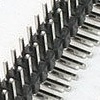
Fit and solder the bus connector, P1. This can either be a right-angled box header or right-angled header pins. The box header is recommended.
Take care to ensure the connector is fitted such that the card will stand vertically when fitted to a backplane. A good method is to just solder two pins, one at each end, and then check it looks correct. Then solder two more, one at each end but in the other row, and check again. At each stage, if necessary, adjust the position by heating the required solder joint and moving the connector slightly. Solder two pins in the middle of the connector and check again. Then solder all the others.

Oscillator
Fit and solder the 7.3727 MHz oscillator, be sure to fit it the correct way around.
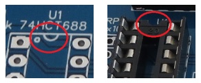
Pin 1 of the oscillator is normally indicated by a ‘sharp’ corner, while the other three corners are rounded.
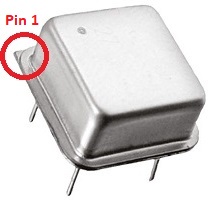
Pin 1 on the circuit board is also indicated by a ‘sharp’ corner, while the other three corners are rounded.

I prefer not to fit a socket for these oscillators as they stick up quite high and have exposed metal on top, increasing the risk of accidental short circuits. Also, they are quite heavy and are only held in the socket by four pins, so additional securing is often needed.
Inspection
Remove any solder ‘splats’ with a brush, such as an old toothbrush.
Visually inspect the soldering for dry joints and shorts.
Clean the flux off with suitable cleaning materials.
Visually inspect again.
Configuration
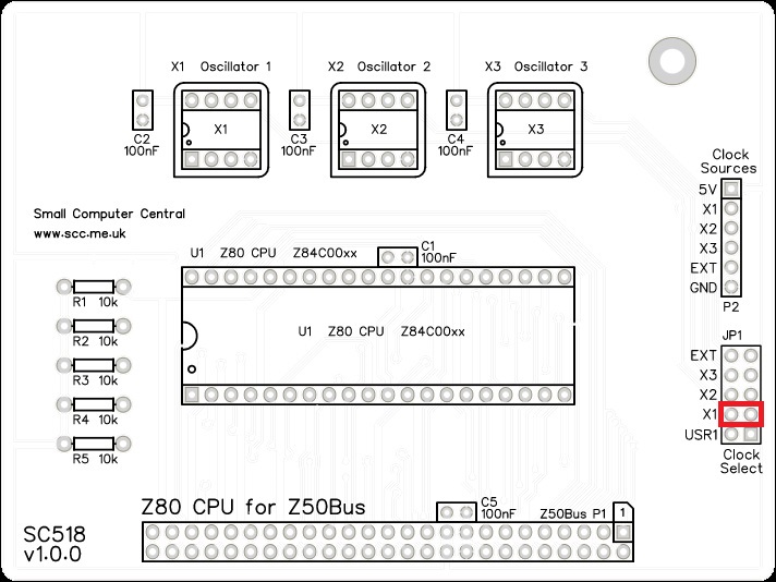
Fit a jumper shunt to JP1, as shown below. This selects X1 as the clock source for the system.
Integrated Circuits
Insert the IC U1 into its socket, taking care to insert it the right way around, as illustrated below. Be careful not to bend any legs over. ICs are usually supplied with the legs slightly spread out making them difficult to insert. It is best to bend the two rows of legs so they are parallel before inserting them. Remember, these components can be damaged by static electricity so if possible earth yourself and the components while handling them.

Notes
- This design is made with the permission of LiNC (designers of the Z50Bus).
- This product is designed for hobby use and is not suitable for industrial, commercial, or safety-critical applications.
- The product contains small parts and is not suitable for young children.
