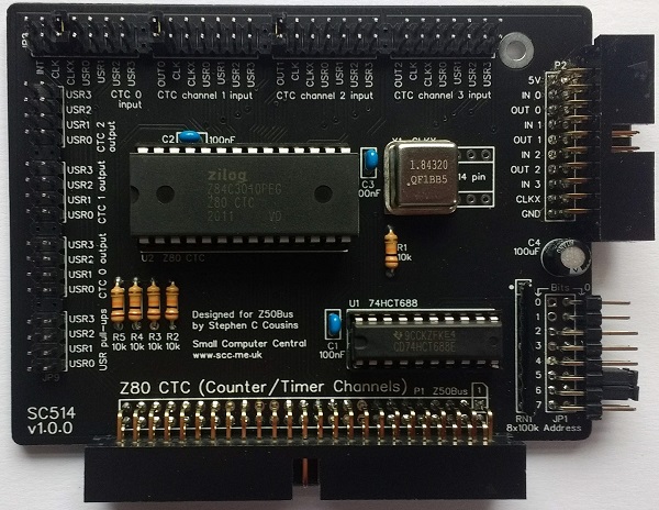
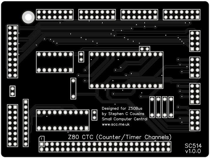
SC514 is a Z80 Counter/Timer Channels (CTC) card designed for Z50Bus.
Documentation
- SC500 – Series Information
- SC514 – Description
- SC514 – Assembly Guide
- SC514 – Parts List
- SC514 – Printed Circuit Board
- SC514 – Support
- SC514 – User Guide
Downloads
Kits
Examples
- SC514 CTC timer demo v1.0 (ZIP) – see SC415 User Guide
Description
SC514 is a Z80 CTC card designed for Z50Bus.
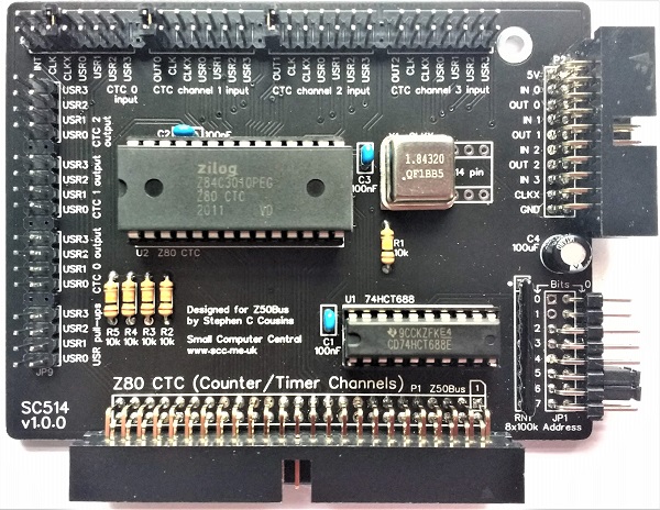
The Z80 Counter/Timer Channels (CTC) integrated circuit has four independently programmable counter/timer channels. Each channel can generate a unique mode 2 interrupt.
Each channel’s input and output can be connected in a variety of ways with jumpers. This includes using the Z50Bus USR pins as either input single sources or output signal destinations. It is also possible to cascade channels to create up to a 32-bit counter timer.
The board includes flexible I/O address decoding allowing the CTC’s base address to be on any 4-byte boundary.
The card includes an oscillator making the card’s functionality independent of the main bus clock frequency, thus allowing compatibility of software across different processor speeds.
The main features of this module are:
- Full Z80 mode 2 interrupt support (IEI/IEO daisy-chain)
- Four independent counter/timer channels
- Ability to generate a clock tick interrupt
- On-board clock option to make it independent of the CPU clock
- Interrupt mode 2 converter for up to 4 devices
Parts List
| Reference | Qty | Component |
| PCB | 1 | SC514, v1.0, PCB |
| C1 to C3 | 3 | Capacitor, ceramic, 100 nF |
| C4 | 1 | Capacitor, electrolytic, 100 µF |
| JP1 | 1 | Header, male, 2 x 8 pin, angled |
| JP2+JP4+JP6+JP8 | 1 | Header, male, 2 row x 31 pin, straight |
| JP3+JP5+JP7+JP9 | 1 | Header, male, 2 row x 19 pin, straight |
| Jumper shunts | 20 | Jumper shunt Two used to pad box header |
| P1 | 1 | Box header, 2 x 25 pin, angled, or Header, male, 2 x 25 pin, angled Box header supplied in kit |
| P2 | 1 | Box header, 2 x 10 pin, angled, or Header, male, 2 x 10 pin, angled Box header supplied in kit |
| R1 to R5 | 5 | Resistor, 10k, 0.25W |
| RN1 | 1 | Resistor network, 8 x 100k, SIL, 9-pin |
| Spacer | 1 | Spacer, 10mm, M3, nylon |
| Screw (for spacer) | 1 | Machine screw, 6mm, M3 |
| U1 | 1 | 74HCT688 |
| U2 | 1 | Z80 CTC, Z84C3008PEG, or Z80 CTC, Z84C3010PEG |
| IC socket 20-pin U1 | 1 | 20-pin PDIP socket |
| IC socket 28-pin U2 | 1 | 28-pin DIP socket |
| X1 | 1 | Oscillator, 1.8432 MHz Solder to PCB recommended |
| X1 socket | 1 | 8-pin DIP socket Socket not recommended Not included in the kit |
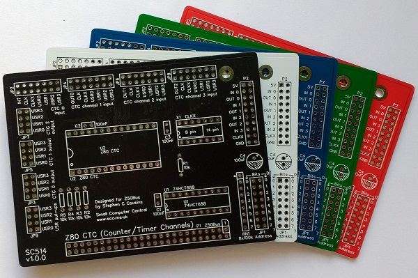
Printed Circuit Board
| Supplier | Website | Ships from |
| Stephen C Cousins | Tindie | UK |
| pcb4diy | pcb4diy.de | Germany |
| pcb4diy | eBay | Germany |
User Guide
SC514 is a Z80 CTC card designed for Z50Bus.
The Z80 Counter/Timer Channels (CTC) integrated circuit has four independently programmable counter/timer channels. Each channel can generate a unique mode 2 interrupt.
Each channel’s input and output can be connected in a variety of ways with jumpers. This includes using the Z50Bus USR pins as either input single sources or output signal destinations. It is also possible to cascade channels to create up to a 32-bit counter timer.
The board includes flexible I/O address decoding allowing the CTC’s base address to be on any 4-byte boundary.
The card includes an oscillator making the card’s functionality independent of the main bus clock frequency, thus allowing compatibility of software across different processor speeds.
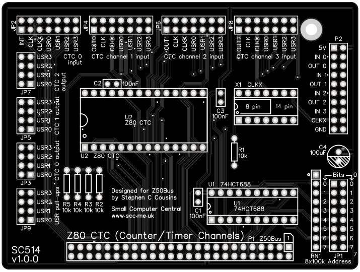
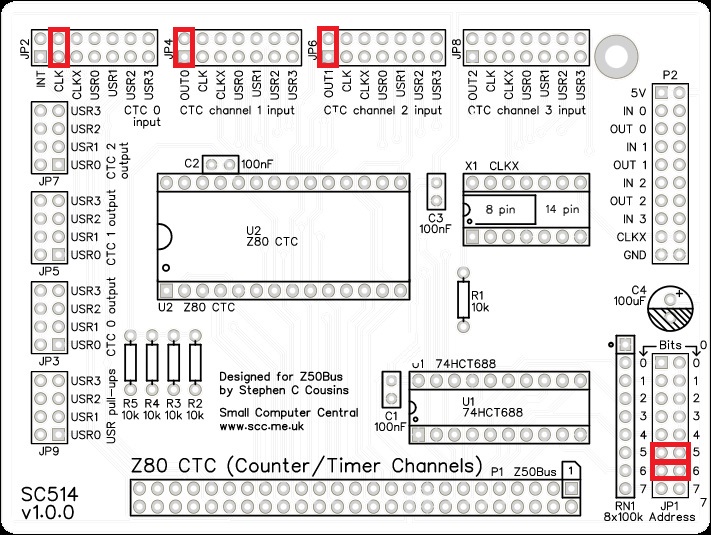
Address select jumpers
The card responds to input/output addresses matching the address set with jumpers. When a jumper shunt is fitted, that bit must be a 1 (high voltage). When the shunt is not fitted, that bit must be a 0 (low voltage).
Header JP1 is the 8 address select jumpers that are labelled with their bit numbers. The card occupies 4 addresses, thus address bits 0 and 1 are not included in the address decoding. The board includes placeholders for bits 0 and 1 for consistency with other cards in the SC500 series. It is suggested that you remove or cut the pins for bits 0 and 1 as a reminder that they are not used.
The recommended base address is currently 60 hex (01100000 binary) when used as part of an SC500 system. This address is selected by fitting jumper shunts for bits 6 and 5. A CTC at this address is not used by any current system software, such as for the system timer or baud rate clock generator.
It is possible to use this card as a system timer by setting the base address to 0x88. Current system software assumes a CTC at this address uses channels 0 and 1 for baud rate clock generators and channels 2 and 3 for the system timer.
Input Jumpers
Each of the four channels has a set of jumpers to select the input source. The available input sources are shown below. Fit a single jumper shunt to one of the positions of each of the sets of jumper header pins labelled “CTC channel # input” (JP2, 4, 6, and 8) to select the required input signal. Alternatively, connect a signal to the required input on connector P2.
| Channel 0 input (JP2) | Channel 1 input (JP4) | Channel 2 input (JP6) | Channel 3 input (JP8) |
| INT | OUT0 | OUT1 | OUT2 |
| CLK | CLK | CLK | CLK |
| CLKX | CLKX | CLKX | CLKX |
| USR0 | USR0 | USR0 | USR0 |
| USR1 | USR1 | USR1 | USR1 |
| USR2 | USR2 | USR2 | USR2 |
| USR3 | USR3 | USR3 | USR3 |
INT = Z50Bus interrupt request signal
OUT0 = CTC channel 0’s output
OUT1 = CTC channel 1’s output
OUT2 = CTC channel 2’s output
CLK = Z50Bus clock signal
CLKX = SC514’s on-board oscillator (typically 1.8432 MHz)
USR0 = Z50Bus user 0 signal
USR1 = Z50Bus user 0 signal
USR2 = Z50Bus user 0 signal
USR3 = Z50Bus user 0 signal
Each channel is 8-bit but the channels can be cascaded by fitting jumper shunts to connect the output of one channel to the input of the next. This allows 16-bit, 24-bit and 32-bit counter/timers to be created.
Output Jumpers
The outputs of the first three channels can optionally be connected to any of the four USR pins on the Z50Bus. This is achieved by fitting a jumper shunt to the header pins labelled “CTC # output” (JP3, 5, and 7).
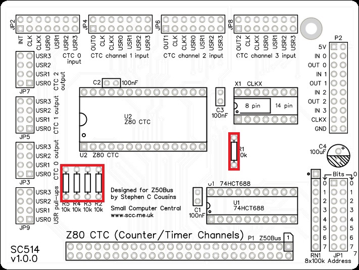
Pull-up Resistors
Each of the Z50Bus USR signals has an optional 10k pull-up resistor. The pull-up resistors are connected by fitting jumper shunts to the jumper header pins labelled “USR pull-ups” (JP9).
Interrupt Mode 2 Converter
One application of this card is to generate Z80 mode 2 interrupts for non-Z80 family devices.
It is desirable to use Z80 mode 2 interrupts but this causes a problem when using devices that can not generate the necessary signals. One solution is to use a Z80 CTC to generate a mode 2 interrupt for such devices. By connecting the interrupt output of the non-Z80 family device to the input of a CTC, it is possible to program the CTC to generate an interrupt when the input signal changes state.
The signal from the non-Z80 family device to the CTC could be connected with a flying lead to connector P2. Alternatively, it could be connected through one of the Z50Bus USR signals.
Example Program
Example – SC514 CTC timer demo v1.0 (ZIP)
This program has been written for the Small Computer Monitor (SCM) running on a system with an SC514 (Z80 CTC card for Z50Bus) set to address 0x60.
This code demonstrates how to generate a periodic mode 2 interrupt using a Z80 CTC.
CTC channel 0 is set to divide the onboard oscillator’s frequency by 256. The onboard oscillator is assumed to be 1.8432 MHz (CLKX) giving a 7200 Hz output from channel 0. ie. 1843200 / 256 = 7200.
CTC channel 1 is set to generate an interrupt every 10 ms (100 Hz). Channel 1’s input is connected to channel 0’s output, thus its input is 7200 Hz. By dividing by 72 the output of channel 1 is 100 Hz.
CTC channel 2 counts the output pulses from channel 1, thus it counts the number of 10 ms events. Note, the counter counts down, not up. Channel 2’s input is connected to channel 1’s output. This is totally optional to the interrupts generated by channel 1.
Channel 1 generates a 10 ms (100 Hz) period mode 2 interrupt.
The required jumper positions for this example are shown below.
Assembly Guide
Important note: How to modify box headers
Experienced builders can just go ahead and populate the board. There shouldn’t be any surprises to catch you out.
This guide assumes you are familiar with assembling circuit boards, soldering, and cleaning. If not, it is recommended you read some of the guides on the internet before continuing.
First check you have all the required components, as listed in the parts list.
Before assembling it is worth visually inspecting the circuit board for anything that looks out of place, such as mechanical damage or apparent manufacturing defects.
If you have a multimeter that measures resistance or has a continuity test function, check there is not a short on the power supply tracks. Connect the probes to each terminal of one of the capacitors, such as C1. This should be an open circuit, not a short.
The picture below shows what a completed SC512 should look like.

Resistors
Fit and solder the 10k resistors, R1 to R5 (shown below in red).
Resistors can be fitted either way around, as they are not polarity dependent.
IC sockets
Fit and solder the IC sockets.
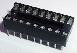
Be sure to fit them with the notch matching the legend on the circuit board, so you do not end up fitting the IC the wrong way around too.

Soldering the oscillator directly to the PCB is recommended, but if you would rather use a socket then fit the socket now.
Resistor network
Fit and solder the 8x100k resistor network, RN1.
The 100k network will be marked 104.
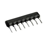
Take care to fit the resistor network the correct way around. Pin 1 is usually marked with a dot. This end is indicated on the PCB and on the illustration below.


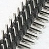
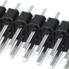
Double row angled header pins
Fit and solder the double row angled header pins, JP1.
This may need to be cut from a longer strip.
Header JP1 is the 6 address select jumpers that are labelled with their bit numbers. The card occupies 4 addresses, thus address bits 0 and 1 are not included in the address decoding. The board includes placeholders for bits 0 and 1 for consistency with other cards in the SC500 series. It is suggested that you remove or cut the pins for bits 0 and 1 as a reminder that they are not used.

Double row straight header pins
Fit and solder the double row angled header pins, JP2 to JP9.
These may need to be cut from a longer strip.
These can be fitted as eight short lengths or two long lengths with pins removed for the gaps between sets. Pins can be pulled out with pliers.

Bus connector and I/O connector
Fit and solder the bus connector (P1) and the I/O connector (P2). These can either be right-angled box headers or right-angled header pins. Box headers are recommended.
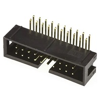

Take care to ensure the bus connector is fitted such that the card will stand vertically when fitted to a backplane. A good method is to just solder two pins, one at each end, and then check it looks correct. Then solder two more, one at each end but in the other row, and check again. At each stage, if necessary, adjust the position by heating the required solder joint and moving the connector slightly. Solder two pins in the middle of the connector and check again. Then solder all the others.

Capacitor 100 nF (0.1 µF)
Fit and solder capacitors, C1 to C3.
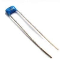
This capacitor can be fitted either way around, as it is not polarity dependent.
The exact value of this component is not critical. The use of very cheap capacitors within the range of about 30 to 200 nF is acceptable.

Capacitor (100uF)
Fit and solder capacitor C4.
It is important to fit this capacitor the right way around. The negative terminal is indicated with a ‘minus’ sign, as illustrated to the right. The negative terminal also has a shorter lead.
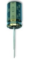
The silkscreen has a plus sign for the positive terminal and a hashed area for the negative terminal.

Oscillator
Fit and solder the 1.8432 MHz oscillator, be sure to fit it the correct way around.
Pin 1 of the oscillator is normally indicated by a ‘sharp’ corner, while the other three corners are rounded.
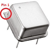
Pin 1 on the circuit board is indicated by a square pad and a small ‘dot’. See illustration below.
The circuit board allows for the use of either a half-size (8-pin DIP style) or a full-size (14-pin DIP style) oscillator. In each case, the component only has 4-pins, one in each corner.

Inspection
Remove any solder ‘splats’ with a brush, such as an old toothbrush.
Visually inspect the soldering for dry joints and shorts.
Clean the flux off with suitable cleaning materials.
Visually inspect again. The importance of visual inspection can not be overstated.
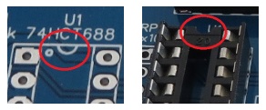
Quick Test
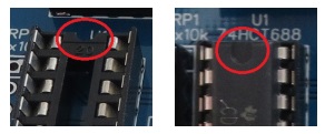
Check for a short on the power supply tracks by measuring the resistance between IC U1 pin 20 and U1 pin 10 (indicated below). This should be an open circuit, not a short. If you are using a digital meter set to measure resistance it will likely take a few seconds for the reading to stabilise as there are now capacitors on the power lines. A reading of more than 100k Ω (100000 ohms) is acceptable.

Integrated circuit
Insert the integrated circuits (ICs) into their sockets, taking care to insert them the right way around, as illustrated below. Be careful not to bend any legs over.
Address select jumpers
The card responds to input/output addresses matching the address set with jumpers. When a jumper shunt is fitted, that bit must be a 1 (high voltage). When the shunt is not fitted, that bit must be a 0 (low voltage).
Header JP1 is the 6 address select jumpers that are labelled with their bit numbers. The card occupies 4 addresses, thus address bits 0 and 1 are not included in the address decoding. The board includes placeholders for bits 0 and 1 for consistency with other cards in the SC500 series. It is suggested that you remove or cut the pins for bits 0 and 1 as a reminder that they are not used.
The recommended base address is currently 60 hex (01100000 binary) when used as part of an SC500 system. This address is selected by fitting jumper shunts for bits 6 and 5. A CTC at this address is not used by any current system software, such as for the system timer or baud rate clock generator.
It is possible to use this card as a system timer by setting the base address to 0x88. Current system software assumes a CTC at this address uses channels 0 and 1 for baud rate clock generators and channels 2 and 3 for the system timer.
You are now ready to give it a try.
Notes
- This design is made with the permission of LiNC (designers of the Z50Bus).
- This product is designed for hobby use and is not suitable for industrial, commercial, or safety-critical applications.
- The product contains small parts and is not suitable for young children.
