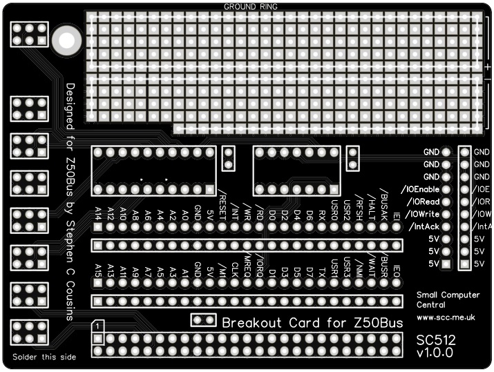
SC512 is a prototyping breakout card designed for Z50Bus.

Documentation
- SC500 – Series Information
- SC512 – Description
- SC512 – Assembly Guide
- SC512 – Parts List
- SC512 – Printed Circuit Board
- SC512 – Support
- SC512 – User Guide
Downloads
Kits
Description
SC512 is a prototyping breakout card designed for Z50Bus.
This has been designed primarily as an aid to prototyping Z50Bus cards with solderless breadboards, although it does also include a prototyping area.

Z50Bus signals to be easily connected to a breadboard with Dupont cables.
The board includes flexible I/O address decoding, so you don’t need to include such circuitry on every prototype. The decoding has jumpers to configure the start address and range. This includes allowing partial decoding with shadow addresses.
The address decoding circuit provides an I/O enable signal (/IOEN) and also separate read and write versions (/IORD and /IOWR). This range of enable signals allows easy interfacing to most I/O devices.
The main features of this card are:
- Easy access to Z50Bus signals
- Flexible address decoding generates /IOWR, /IORD and /IOEN
- Connection to solderless breadboards with Dupont cables
Parts List
| Reference | Qty | Component |
| PCB | 1 | SC512, v1.0, PCB |
| C1 to C3 | 3 | Capacitor, ceramic, 100 nF |
| JP1 to JP8 | 8 | Header, male, 2 row x 3 pin, straight |
| JP1 shunt | 8 | Jumper shunt |
| P1 | 1 | Box header, 2 x 25 pin, angled, or Header, male, 2 x 25 pin, angled |
| P2 and P3 | 2 | Header, male, 1 row x 25 pin, straight |
| P4 | 1 | Header, male, 1 row x 10 pin, straight |
| Spacer | 1 | Spacer, 10mm, M3, nylon |
| Screw (for spacer) | 1 | Machine screw, 6mm, M3 |
| U1 | 1 | 74HCT688 |
| U2 | 1 | 74HCT32 |
| IC socket 20-pin U1 | 1 | 20-pin PDIP socket |
| IC socket 14-pin U2 | 1 | 14-pin PDIP socket |
Printed Circuit Board
| Supplier | Website | Ships from |
| Stephen C Cousins | Tindie | UK |
| pcb4diy | pcb4diy.de | Germany |
| pcb4diy | eBay | Germany |


User Guide
Prototyping with SC512 can be either using SC512 to breakout signals to a solderless breadboard (with Dupont wires) or to create a stand-alone prototype with components mounted on the matrix area of the card.
This card includes flexible address decoding, with each address bit (A1 to A7) matching the conditions set with jumpers JP1 to JP7. The required state of the Z80 M1 signal is set with JP8. Note that A0 is not included in the address decoding, so the minimum number of I/O addresses occupied by the card is two addresses.
In each case, the required condition of each signal can be high (1), low (0), or don’t care (1 or 0). This provides very flexible address decoding and even allows you to create ghost addresses, which are common when compromised address decode is to be used by a design.
The illustration below shows the jumper shunt positions for address decoding of a device that occupies the address range 0x20 to 0x27. The required address bits for this range are:
A7=0, A6=0, A5=1, A4=0, A3=0, A2=0 or 1, A1=0 or 1, A0=0 or 1
To select a ‘0’ as the required state of an address bit, fit a jumper shunt to position “0” for that signal. For a ‘1’ fit the shunt to position “1”. If the signal can be in either state, fit a jumper shunt in the “don’t care” (middle) position.
In this example, we have set the required state of the M1 signal to “1”. This is the usual state required by I/O devices unless the device is a Z80 family IC, such as a Z80 PIO, or the address decoding also includes the RD or WR signal. This requirement is to stop a device from being enabled during a Z80 interrupt acknowledge cycle.

Note that A0 is always set as “don’t care”.
This card generates a device enable signal (/IOEnable), a read from the device signal (/IORead), and a write to the device signal (/IOWrite). It also generates an interrupt acknowledge signal (/IntAck). All these signals are available on pin header, P4.
All the Z50Bus signals are available on either P2 or P3,
Assembly Guide
Important note: How to modify box headers
As this card is only useful for prototyping, it is assumed the user is familiar with assembling circuit boards, and therefore a detailed assembly guide is not required.
The picture below shows what a completed SC512 should look like.
Notes
- This design is made with the permission of LiNC (designers of the Z50Bus).
- This product is designed for hobby use and is not suitable for industrial, commercial, or safety-critical applications.
- The product contains small parts and is not suitable for young children.
