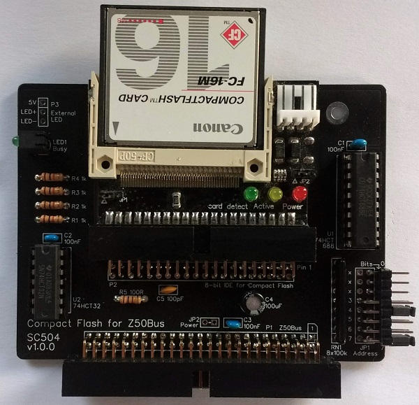
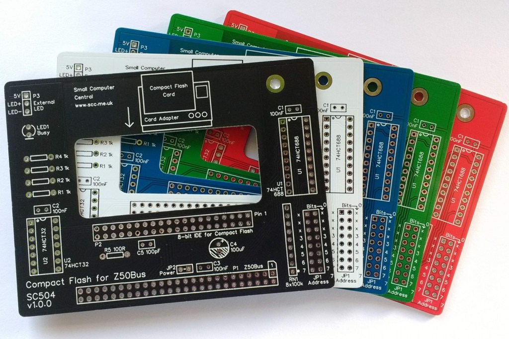
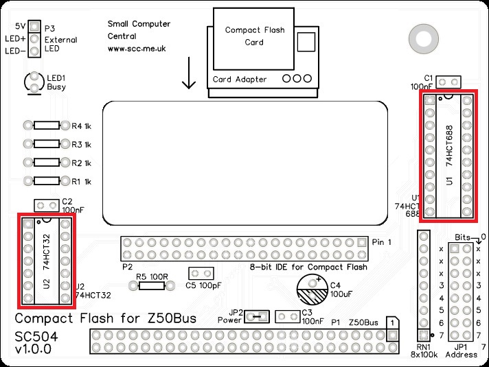
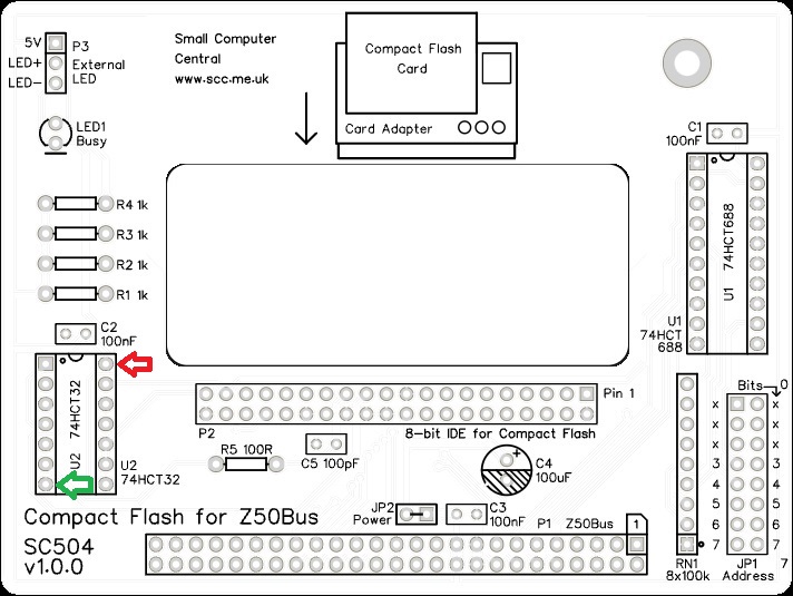
SC504 is a Compact Flash interface designed for Z50Bus.
See notes about the Compact Flash adapter.
Documentation
- SC500 – Series Information
- SC504 – Assembly Guide
- SC504 – Description
- SC504 – Parts List
- SC504 – Printed Circuit Board
- SC504 – Support
- SC504 – User Guide
Downloads
Kits
Description
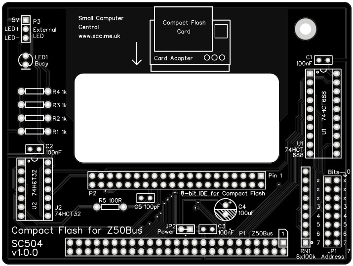
This card provides an 8-bit IDE interface via a 40-pin male header. In theory, you could connect other IDE devices, not just the recommended Compact Flash adapter module (shown right).
As this is a very simple interface, which uses the processor bus directly, without buffering, the IDE interface should not be extended for than a few inches and only carefully selected devices should be connected. In general, it is best to only use this interface to connect a Compact Flash card.
The card has the following features:
- Z50Bus compatible (“Standard” card size 100mm x 75mm, but with a cut-out for the Compact Flash adapter module)
- Tight address decoding
- Flexible I/O address selection
- Optional power to IDE connector
- Activity LED
User Guide
This card provides an 8-bit IDE interface via a 40-pin male header. In theory, you could connect other IDE devices, not just the recommended Compact Flash adapter module (shown above).
As this is a very simple interface, which uses the processor bus directly, without buffering, the IDE interface should not be extended for than a few inches and only carefully selected devices should be connected. In general, it is best to only use this interface to connect a Compact Flash card.
It is recommended that this card be placed close to the CPU card.
Not all Compact Flash cards are compatible with this simple 8-IDE interface. Older cards tend to be best. Large capacity, more modern cards are designed for very fast operation. This means very sharp edges on signals generated by the Compact Flash card. These edges can cause reliability problems with this simple, bus based interface.
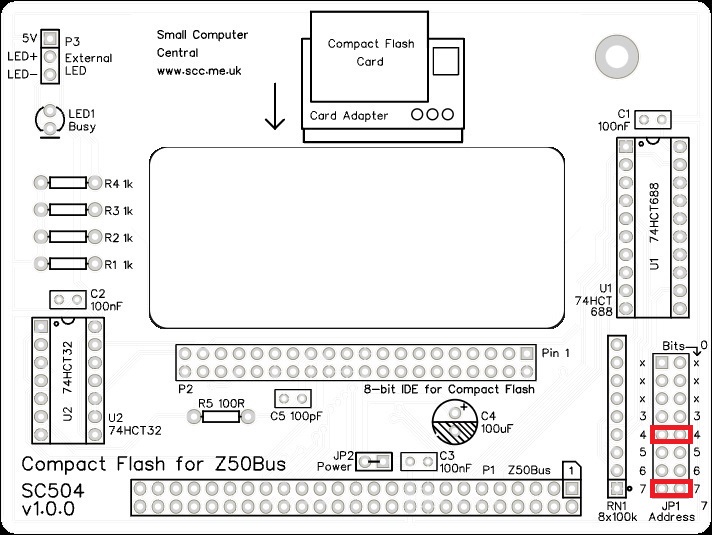
Address
The I/O address of this card can be set with jumper, JP1. The card occupies 8 I/O address, thus address bits 0 to 2 are not included in the address decoding.
Most new software will assume the I/O address for this card is 0x90 (binary 10010000). The other likely address is 0x10 (binary 00010000).
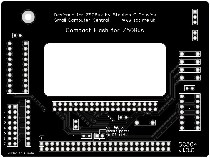
Power
The device plugged into P2 (20 pin, 8-bit IDE) can be either self-powered or it can take power from SC504. The recommended Compact Flash adapter module must be powered from SC504.
As it is very likely the connected device will need to be powered from SC504, JP2 has a track connecting its two pads. Thus the jumper header and jumper shunt are optional. If fitted, the track between the pads of JP2 must be cut. This track is on the solder side of the PCB.
Software
If the system is running RomWBW (which includes CP/M) the Compact Flash can be initialised for use with the CLRDIR command. CP/M does not need to be installed on the Compact Flash card as RomWBW is a ROM based operating system that includes CP/M. With recent releases of RomWBW you may need to use FDISK80 first.
If the system is running plain CP/M (not RomWBW) the Compact Flash card needs to be prepared before use. Instructions to install CP/M 2.2 on to a Compact Flash card can be found here.
The version of CP/M for this card, together with a Z80 processor card, is detailed here.
If you are using the Small Computer Monitor firmware then CP/M can be loaded and started from a suitably prepared Compact Flash card with the command “CPM”.
Parts List
| Reference | Qty | Component |
| PCB | 1 | SC504, v1.0, PCB |
| C1 to C3 | 3 | Capacitor, ceramic, 100 nF |
| C4 | 1 | Capacitor, electrolytic, 100 µF |
| C5 | 1 | Capacitor, ceramic, 100 pF |
| JP1 | 1 | Header, male, 2 x 8 pin, angled |
| JP2 | 0 | Linked with thin track Header pins not included in the kit |
| Jumper shunts | 5 | Jumper shunt |
| LED1 | 1 | LED, green, 3mm, angled |
| P1 | 1 | Box header, 2 x 25 pin, angled, or Header, male, 2 x 25 pin, angled |
| P2 | 1 | Box header, 2 x 20 pin, angled, angled, or Header, male, 2 x 20 pin, angled |
| P3 | 0 | Only required for external LED Header pins not included in the kit |
| R1 to R4 | 4 | Resistor, 1k, 0.25W |
| R5 | 1 | Resistor, 100R, 0.25W |
| RN1 | 1 | Resistor network, 8 x 100k, SIL, 9-pin |
| Spacer | 1 | Spacer, 10mm, M3, nylon |
| Screw (for spacer) | 1 | Machine screw, 6mm, M3 |
| U1 | 1 | 74HCT688 |
| U2 | 1 | 74HCT32 |
| IC socket 14-pin U2 | 1 | 14-pin PDIP socket |
| IC socket 20-pin U1 | 1 | 20-pin PDIP socket |
Printed Circuit Board
| Supplier | Website | Ships from |
| Stephen C Cousins | Tindie | UK |
| pcb4diy | pcb4diy.de | Germany |
| pcb4diy | eBay | Germany |
Assembly Guide
Important note: How to modify box headers
Important note: Compact Flash adapters
Experienced builders can just go ahead and populate the board. There shouldn’t be any surprises to catch you out.
This guide assumes you are familiar with assembling circuit boards, soldering, and cleaning. If not, it is recommended you read some of the guides on the internet before continuing.
First check you have all the required components, as listed in the parts list.
Before assembling it is worth visually inspecting the circuit board for anything that looks out of place, such as mechanical damage or apparent manufacturing defects.
If you have a multimeter that measures resistance or has a continuity test function, check there is not a short on the power supply tracks. Connect the probes to each terminal of one of the capacitors, such as C1. This should be an open circuit, not a short.
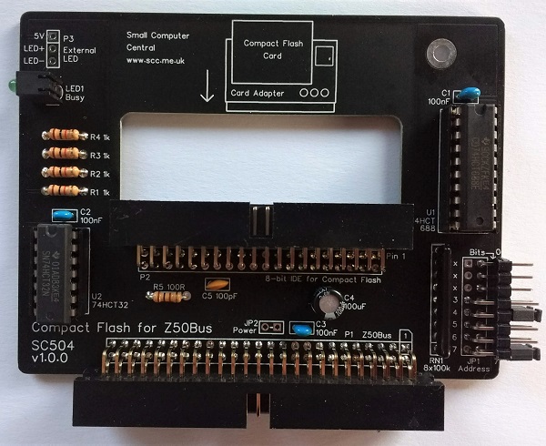
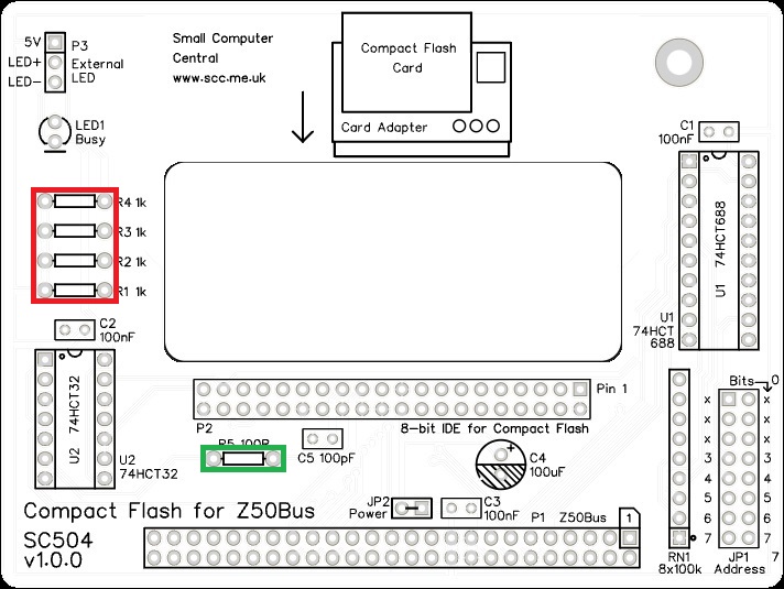
The picture below shows what a completed SC504 should look like.
Resistors
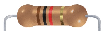
Fit and solder the 1k resistors, R1 to R4, shown below in red.
Fit and solder the 100R resistor, R5, shown below in green.
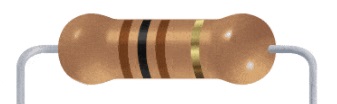
Resistors can be fitted either way around, as they are not polarity dependent.
IC sockets
Fit and solder the IC sockets.
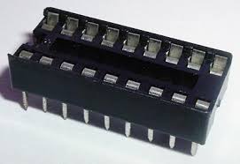
Be sure to fit them with the notch matching the legend on the circuit board, so you do not end up fitting the IC the wrong way around too.
Resistor network
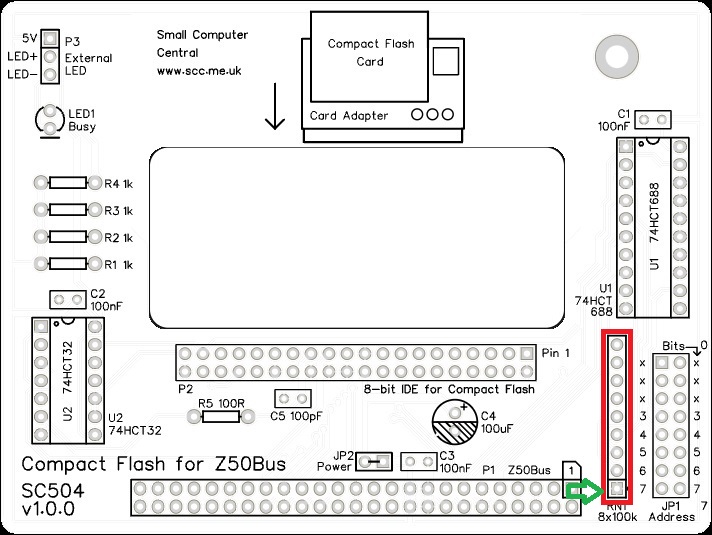
Fit and solder the 8x100k resistor network, RN1.
The 100k network will be marked 104.
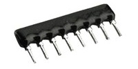
Take care to fit the resistor network the correct way around. Pin 1 is usually marked with a dot. This end is indicated on the PCB and on the illustration below.
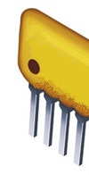
Light Emitting Diode (LED)
Fit and solder green LED, LED1.
If using an angled LED the polarity is predefined and matches the PCB.
If using standard LEDs care must be taken to ensure they are fitted the correct way around.
It is important to fit the LED the correct way around. LEDs usually have a small flat side to indicate the cathode (the negative end). This should be positioned to match the flat side shown on the circuit board (illustrated to the right). Also, the cathode pin on the LED is usually shorter than the other pin (the Anode).

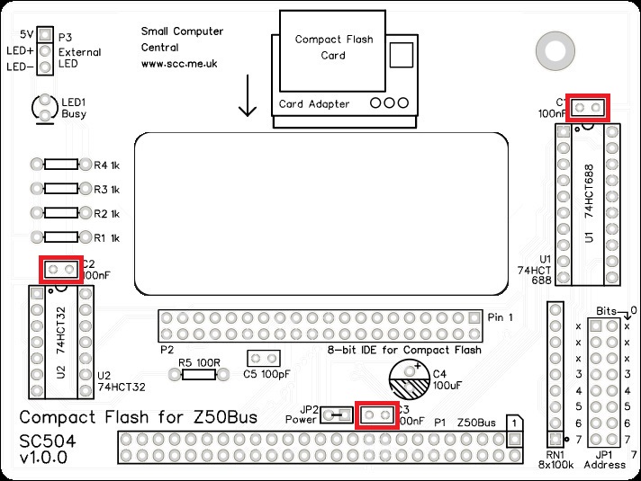
Capacitors (100 nF)
Fit and solder the 100 nF capacitors, C1 to C3.
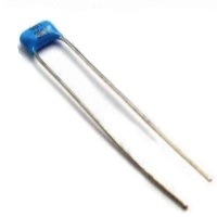
These can be fitted either way around as they are not polarity dependent.
The exact value of this component is not critical. The use of very cheap capacitors within the range of about 30 to 200 nF is acceptable.
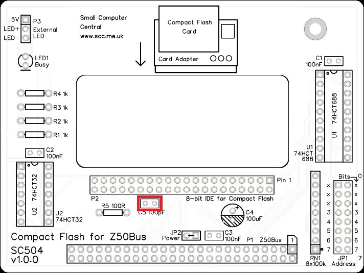
Capacitor (100 pF)
Fit and solder the 100 pF cacacitor, C5.
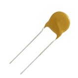
These can be fitted either way around as they are not polarity dependent.
Double row angled header pins
Fit and solder the double row angled header pins, JP1.
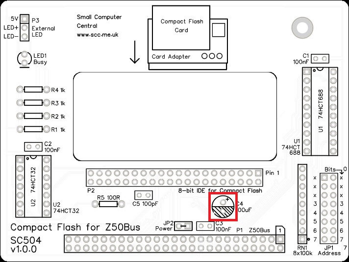
Capacitor (100uF)
Fit and solder capacitor, C4.
It is important to fit this capacitor the right way around. The negative terminal is indicated with a ‘minus’ sign, as illustrated to the right. The negative terminal also has a shorter lead.
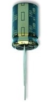
The silkscreen has a plus sign for the positive terminal and a hashed area for the negative terminal.
IDE connector
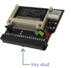
Fit and solder the IDE connector, P2. This can either be a right-angled box header or right-angled header pins. The box header is recommended.
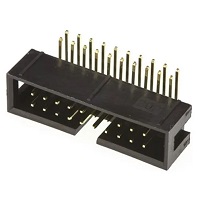

If you fit the box header you will need to cut or file the key stud off the compact flash adapter, as the box header’s key slot is on the wrong side for this particular application.
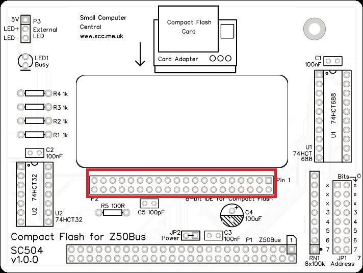
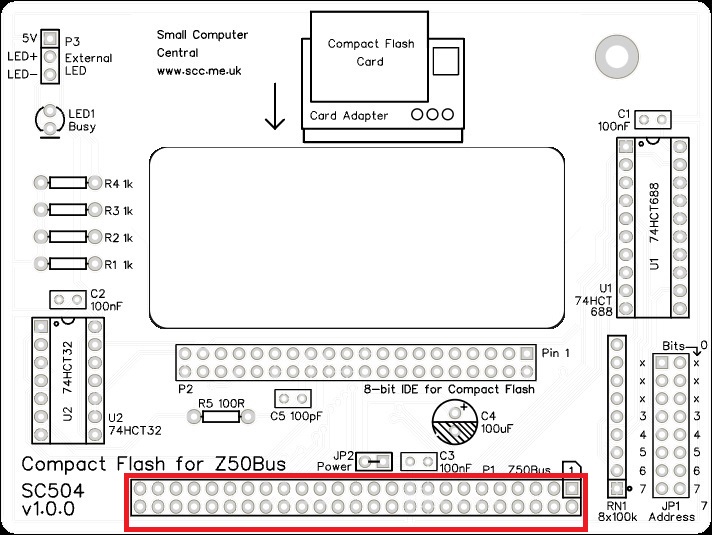
Bus connector
Fit and solder the bus connector, P1. This can either be a right-angled box header or right-angled header pins. The box header is recommended.
Take care to ensure the connector is fitted such that the card will stand vertically when fitted to a backplane. A good method is to just solder two pins, one at each end, and then check it looks correct. Then solder two more, one at each end but in the other row, and check again. At each stage, if necessary, adjust the position by heating the required solder joint and moving the connector slightly. Solder two pins in the middle of the connector and check again. Then solder all the others.
JP2 and P3
These are not included in the kit.
Inspection
Remove any solder ‘splats’ with a brush, such as an old toothbrush.
Visually inspect the soldering for dry joints and shorts.
Clean the flux off with suitable cleaning materials.
Visually inspect again. The importance of visual inspection can not be overstated.
Quick Test
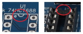
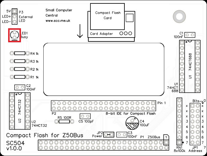
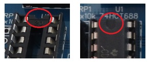
Check for a short on the power supply tracks by measuring the resistance between IC U2 pin 14 and U1 pin 7 (indicated below). This should be an open circuit, not a short. If you are using a digital meter set to measure resistance it will likely take a few seconds for the reading to stabilise as there are now capacitors on the power lines. A reading of more than 100k Ω (100000 ohms) is acceptable.
Integrated circuit
Insert the integrated circuits (ICs) into their sockets, taking care to insert them the right way around, as illustrated below. Be careful not to bend any legs over.
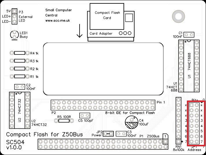
Address select jumpers
The card responds to input/output addresses matching the address set with jumpers. When a jumper shunt is fitted, that bit must be a 1 (high voltage). When the shunt is not fitted, that bit must be a 0 (low voltage).
Header JP1 is the 5 address select jumpers which are labelled with their bit numbers. The card occupies 8 addresses, thus address bits 0, 1, and 2 are not included in the address decoding. The board includes place holders for bits 0, 1, and 2 for consistency with other cards in the SC500 series. It is suggested that you remove or cut the pins for bits 0, 1, and 2 as a reminder that they are not used.
Most new software will assume the I/O address for this card is 0x90 (binary 10010000). The other likely address is 0x10 (binary 00010000).
You are now ready to give it a try.
Notes
- This design is made with the permission of LiNC (designers of the Z50Bus).
- This product is designed for hobby use and is not suitable for industrial, commercial, or safety-critical applications.
- The product contains small parts and is not suitable for young children.
