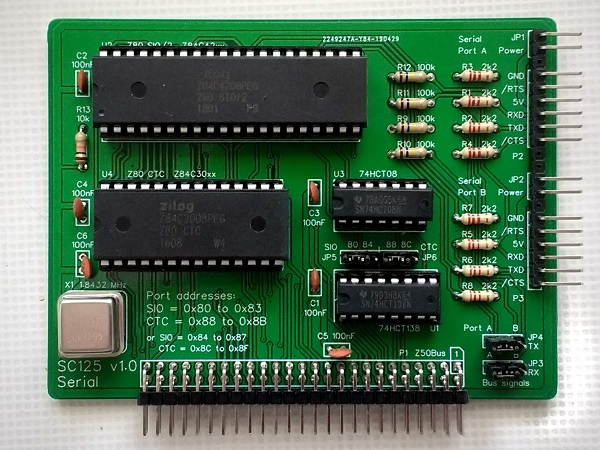
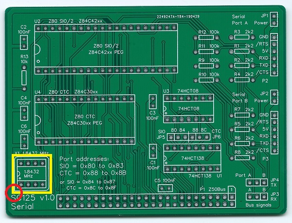
SC125 is a serial interface and timer card for the Z50Bus.
SC511 is a later version of this design
Downloads
Suppliers
- SC125 – Kit (Tindie) – discontinued (replaced with SC511)
- SC125 – PCB (Tindie) – while stocks last
Examples
Older Versions
- none
Description
The SC125, serial and timer card houses a Z80 SIO chip, which provides two TTL serial ports for use with FTDI style serial adapter cables, and a Z80 CTC, which has four counter/timer channels.
The main features of this card are:
- Z50Bus compatible (“Standard” card size 100mm x 75mm)
- Full Z80 mode 2 interrupt support (IEI/IEO daisy-chain)
- Interrupt look-ahead circuit
- Two TTL serial ports for use with FTDI serial adapter cables
- Software control of baud rate for both ports
- On-board oscillator for independence from CPU clock rate
- Clock tick timer
- Two I/O address options
- Optional connection of either port to Z50Bus RX/TX pins
User Guide
The SC125, serial and timer card houses a Z80 SIO chip, which provides two TTL serial ports for use with FTDI style serial adapter cables, and a Z80 CTC, which has four counter/timer channels.

Powering the system
Fitting jumper shunts to headers JP1 and/or JP2 connects the FTDI style 5 volt serial port’s power pin to SC125’s 5 volt supply. This enables the retro computer system to be powered from the serial port, or a device connected to the serial port to be powered from SC125.
Alternatively, power can be supplied from the Z50Bus.
Do not attempt to power the system from two different sources. If the system is not being powered from a serial port, then only fit a jumper shunt to JP1 or JP2 if the serial device is being powered from the system.
Serial on the Z50Bus
The Z50Bus has two lines dedicated to a serial interface. This enabled two cards to communicate via the bus rather than having to have additional cables between the cards.
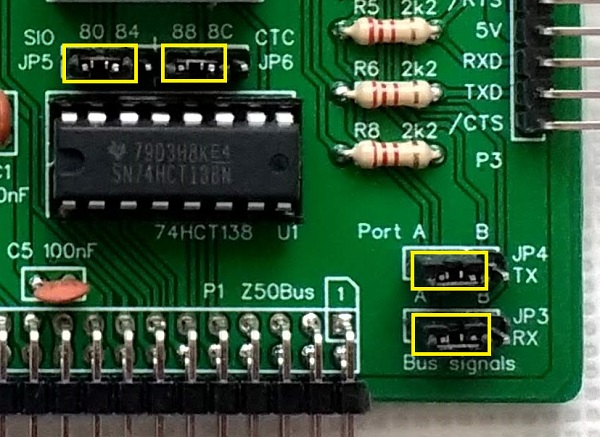
Jumpers JP3 and JP4 enable one of the serial ports to be connected to the Z50Bus RX and TX lines. Each jumper has two positions: A and B. Position A links the port A signals to the bus, while position B is for the port B signals. Leave the jumper shunts off to isolate this card’s RXD and TXD signals from the Z50Bus.
Address Selection
Jumpers JP5 and JP6 allow the address ranges of the SIO and CTC chips to each be set to one of two options. Each chip occupies four I/O addreses. The addresses should be set to either:
| Card | SIO | CTC |
| Primary | 0x80 to 0x83 | 0x88 to 0x8B |
| Secondary | 0x84 to 0x87 | 0x8C to 0x8F |
The primary addresses are the defaults supported by the current firmware. A second card can be added to the system with the secondary addresses selected, but there is not currently any software to support this.
The illustration below shows the default positions for the jumpers shunts on JP3 to JP6.
Serial Ports
Two FTDI style 5 volt serial ports are provided at P2 and P3.
| Pin | Function |
| 1 | Ground (GND) |
| 2 | Request To Send (RTS) output from the card |
| 3 | Vcc (5V) |
| 4 | Recieve Data (RxD) input to the card |
| 5 | Transmit Data (TxD) output from the card |
| 6 | Clear To Send (CTS) input to the card |
The serial ports settings depend on the firmware or software being run. Typically these are:
| Setting | Port A | Port B |
| Baud rate | 115200 | 9600 |
| Data bits | 8 | 8 |
| Stop bits | 1 | 1 |
| Parity | None | None |
| Flow control | None | None |
Current firmware assumes the use of serial port A as the default console device.
Counter / Timer
The Z80 CTC is a four channel counter/timer interface. The channels are used as follows:
- Channel 0: Serial port A baud rate clock
- Channel 1: Serial port B baud rate clock
- Channel 2 and 3: Clock tick generator/timer
The output of channel 2 is connected to the input of channel 3. This makes of a flexible clock tick generator or timer.
For full details search for Z84C30 datasheet or the Zilog Z80 Family CPU Peripherals User Manual (UM0081).
Clock Source
This card has its own oscillator as a clock source for the CTC, making the serial port and timer functions independent of the CPU’s main clock.
Parts List
| Reference | Qty | Component |
| PCB | 1 | SC125, v1.0, PCB |
| C1 to C6 | 6 | Capacitor, ceramic, 100 nF |
| JP1 and JP2 | 2 | Header, male, 1 x 2 pin, angled |
| JP3 and JP4 | 2 | Header, male, 1 x 3 pin, straight |
| JP5 plus JP6 | 1 | Header, male, 1 x 6 pin, straight |
| JP1 to JP6 | 6 | Jumper shunt |
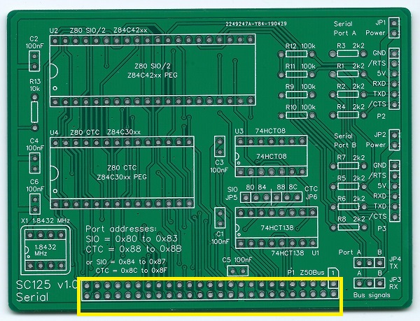
| P1 | 1 | Header, male, 2 x 25 pin, angled |
| P2 and P3 | 2 | Header, male, 1 x 6 pin, angled |
| R1 to R8 | 8 | Resistor, 2k2, 0.25W |
| R9 to R12 | 4 | Resistor, 100k, 0.25W |
| R13 | 1 | Resistor, 10k, 0.25W |
| U1 | 1 | 74HCT138 |
| U1 socket | 1 | 16-pin DIP socket |
| U2 | 1 | Z80 SIO/2, Z84C4208PEG |
| U2 socket | 1 | 40-pin DIP socket |
| U3 | 1 | 74HCT08 |
| U3 socket | 1 | 14-pin DIP socket |
| U4 | 1 | Z80 CTC, Z84C3008PEG |
| U4 socket | 1 | 28-pin DIP socket |
| X1 | 1 | Oscillator, 1.8432 MHz |
| X1 socket | 1 | 8-pin DIP socket |
Printed Circuit Board


| Part number | Links |
| Tindie: SC125 | PCB only |
| Tindie: SC125 | Complete kit – discontinued |
| EasyEDA: SC125 | PCB design files |
| Gerbers: SC125 | Gerber files |
Assembly Guide
Experienced builders can just go ahead and populate the board. There shouldn’t be any surprises to catch you out.
This guide assumes you are familiar with assembling circuit boards, soldering, and cleaning. If not, it is recommended you read some of the guides on the internet before continuing.
First check you have all the required components.
Before assembling it is worth visually inspecting the circuit board for anything that looks out of place, such as mechanical damage or apparent manufacturing defects.
If you have a multimeter that measures resistance or has a continuity test function, check there is not a short on the power supply tracks. Connect the probes to each terminal of one of the capacitors, such as C1. This should be an open circuit, not a short.
The picture below shows what a completed SC125 Serial and timer card should look like.

Resistors
Fit and solder the eight 2k2 resistors, R1 to R8 (shown below in yellow).

Fit and solder the four 100k resistors, R9 to R12 (shown below in red).

Fit and solder the 10k resistor, R13 (shown below in blue).

These can be fitted either way around as they are not polarity dependent.

IC sockets
Fit and solder the IC sockets for U1 to U4 (shown below in yellow).
You may wish to fit a socket for oscillator X1 (shown below in red). My preference is to solder this component as I like low profile boards.
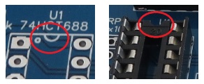
Be sure to fit them with the notch matching the legend on the circuit board, so you do not end up fitting the IC the wrong way around too.

Serial header
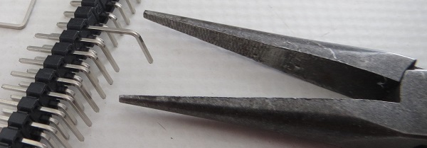
Fit and solder the serial port header pins, P2, P3, JP1 and JP2.
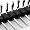
You can either fit these as a single continuous strip, by pulling out the unwanted pins with pliers, or you can cut the strip into the correct side for each header.

Bus header
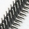
Fit and solder the Z50Bus header pins, P1 (shown below in yellow).
Jumper pins
Fit and solder jumper header pins, JP3 and JP 4 (shown below in yellow).
Fit and solder jumper header pins, JP5 and JP6 (shown below in red).
These can be fitted as a single strip of 6 pins.


Capacitors
Fit and solder the six 100 nF capacitors, C1 to C6 (shown below in yellow).


Oscillator
If you decided to solder the 1.8432 MHz oscillator, be sure to fit it the correct way around.
Pin 1 of the oscillator is normally indicated by a ‘sharp’ corner, while the other three corners are rounded.
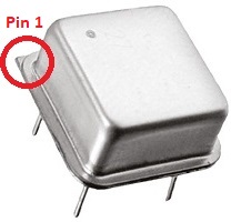
Pin 1 on the circuit board is also indicated by a ‘sharp’ corner, while the other three corners are rounded.

Inspection
Remove any solder ‘splats’ with a brush, such as an old toothbrush.
Visually inspect the soldering for dry joints and shorts.
Clean the flux off with suitable cleaning materials.
Visually inspect again.
With a suitable FTDI style TTL level serial to USB adapter connected from P2 to a powered USB socket, and a jumper shunt fitted to JP1, check the supply voltage on this circuit board between U3 pin 7 and U3 pin 14. This should be 4.5 to 5.5 volts, preferably 4.75 to 5.25 volts. Unplug the serial adapter.
Integrated circuits
Insert the ICs into their sockets, taking care to insert them the right way around, as illustrated below. Be careful not to bend any legs over.

If you fitted a socket for the oscillator, X1, fit the oscillator now.
Test
Fit a jumper shunt to JP5 and another to JP6, in the positions shown below in red. These select the default address for the SIO and CTC chips.
If the system is to be powered from one of the serial ports, fit a jumper shunt in one of the positions indicated below in yellow. The default port is normally port A, so JP1 is the most likely position to fit a jumper shunt.
Do not attempt to power the system from two different sources. If the system is not being powered from a serial port, then only fit a jumper shunt to JP1 or JP2 if the serial device is being powered from the system.
The jumpers shown in blue are optional. They are only needed if you wish to connect one of the serial ports to the Z50Bus RX and TX lines. To connect serial port A to the bus lines, fit the shunts in the positions shown below in red.

You are now ready to play!
Plug this card and a processor card, such as SC118, into a suitable backplane. Connect an FTDI style serial to USB adapter from serial port A (P2) to a computer running a terminal emulation program. The terminal should be configured for 115200 baud, 8 data, 1 stop, no parity. Flow control can be either Off, or hardware RTS/CTS.
Turn the power on to the system. The terminal should show something similar to the illustration below.

Fault Finding
Check there are no chips with bent legs and thus not making contact with their socket, carefully inspect all soldering, check all the chips are inserted the right way around, check all the components are in the right place.
With a suitable FTDI style TTL level serial to USB adapter connected from P2 to a powered USB socket, check the supply voltage on this circuit board between, say, U3 pin 7 and U4 pin 14. This should be 4.5 to 5.5 volts, preferably 4.75 to 5.25 volts.
If your system is running the Small Computer Monitor and you have a means of displaying the self-test results, typically an LED output, check if the serial port has been detected. See the processor card and SCM documentation for details.
If the serial port has not been detected, the problem is probably one of the signals from the Z50Bus to the SIO.
If the serial port has been detected, the main bus connections and SIO chip are probably good. Remove the card from the backplane. Connect a powered FTDI style cable to port B header (P3) and jumper shunts to JP1 and JP2. Now check these voltages on port A header (P2):
- Pin 1, GND, less than 0.1 volts
- Pin 2, /RTS, more than 4.5 volts
- Pin 3, 5V, more than 4.5 volts
- Pin 4, RXD, more than 4.5 volts
- Pin 5, TXD, more than 4.5 volts
- Pin 6, /CTS, less than 0.4 volts
If you have a logic probe or oscilloscope, check the output of the oscillator (X1). This should be 1.8432 MHz.
Circuit Explained
The SC125, serial and timer card houses a Z80 SIO chip, which provides two TTL serial ports for use with FTDI style serial adapter cables, and a Z80 CTC, which has four counter/timer channels.
C1 to C6 (100 nF)
These capacitors provide power supply decoupling (or bypass). The fast switching in digital circuits creates spikes on the power supply lines which are suppressed with decoupling capacitors placed at key points on the circuit board.
JP1 and JP2
Fitting jumper shunts to these headers connects the FTDI style 5 volts serial port’s power pin to SC125’s 5 volt supply. This enables the retro computer system to be powered from the serial port, or a device connected to the serial port to be powered from SC125.
Do not attempt to power the system from two different sources. If the system is not being powered from a serial port, then only fit a jumper shunt to JP1 or JP2 if the serial device is being powered from the system.
JP3 and JP4
These jumpers enable one of the serial ports to be connected to the Z50Bus RX and TX lines. Each jumper has two positions: A and B. Position A links the port A signals to the bus, while position B is for the port B signals. Leave the jumper shunts off to isolate this card’s RXD and TXD signals from the Z50Bus.
JP5 and JP6
These jumpers allow the address ranges of the SIO and CTC chips to each be set to one of two options. Each chip occupies four I/O addreses. The addresses should be set to either:
- Primary: SIO = 0x80 to 0x83, CTC 0x88 to 0x8B
- Secondary: SIO = 0x84 to 0x87, CTC 0x8C to 0x8F
The primary addresses are the default supported by the current firmware. A second card can be added to the system with the secondary addresses selected, but there is not currently any software to support this.
P1
This is the Z50Bus connector.
P2 and P3
Serial ports A and B are connected via P2 and P3. These are FTDI style 5 volt serial ports.
| Pin | Function |
| 1 | Ground (GND) |
| 2 | Request To Send (RTS) output from the card |
| 3 | Vcc (5V) |
| 4 | Recieve Data (RxD) input to the card |
| 5 | Transmit Data (TxD) output from the card |
| 6 | Clear To Send (CTS) input to the card |
R1 to R8 (2k2)
These provide current limiting between the SC125 serial card and the connected serial device (eg. PC or terminal), providing protection for when one is powered and the other is not.
R9 to R12 (100k)
The resistors provide pull up and pull down for the serial port inputs, thus holding them in known states when no device is connected.
R13 (10k)
This provides a pull-up for the Z80 interrupt daisy chain signal IEI. This is needed to ensure this card can generate interrupts when this input is not connected to a valid IEO signal.
Most simple Z50Bus systems will not have multiple cards using Z80 mode 2 interrupts. By pulling this input high via a resistor it avoids the need to consider the daisy-chain when fitting cards to a backplane, whilst allowing a full mode 2 implementation when required.
U1 (74HCT138)
The 74HCT138 provides address decoding for both the SIO and the CTC chips.
U2 (Z80 SIO)
The Z80 SIO is a dual channel serial interface.
For full details search for Z84C40 datasheet or the Zilog Z80 Family CPU Peripherals User Manual (UM0081).
U3 (74HCT08)
The 74HCT08 provides a very basic interrupt look-ahead function. This reduces the time it takes for the daisy-chain to stabilise, allowing more devices in the chain.
U4 (Z80 CTC)
The Z80 CTC is a four channel counter/timer interface. The channels are used as follows:
- Channel 0: Serial port A baud rate clock
- Channel 1: Serial port B baud rate clock
- Channel 2 and 3: Clock tick generator/timer
The output of channel 2 is connected to the input of channel 3. This makes of a flexible clock tick generator or timer.
For full details search for Z84C30 datasheet or the Zilog Z80 Family CPU Peripherals User Manual (UM0081).
X1 (1.8432 MHz)
This oscillator a clock source for the CTC which is independent of the CPU’s main clock. The CTC uses this to generate baud rate clocks for the SIO and a flexible timer.
By removing the oscillator and linking the oscillator socket’s pins 5 and 6, the CPU clock can be used as the CTC clock source. This will, however, need matching software.
