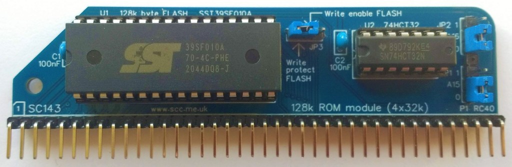
SC143 is a ROM module designed for the RC2014 bus.
- SC143 – Forum (rc2014)
- SC143 – Forum (retro-comp)
- SC143 – Kit contents sheet (PDF)
- SC143 – Schematic v1.0 (PDF)
- SC143 – Gerber files (ZIP)
Suppliers
| Kits | Website | From | Currency |
| Small Computers Direct | SCDirect | UK | GBP |
| Stephen C Cousins | Tindie | UK | USD |
| PCBs | Website | From | Currency |
| Small Computers Direct | SCDirect | UK | GBP |
| Stephen C Cousins | Tindie | UK | USD |
| Assembled and Tested | Website | From | Currency |
| Not available | |||
| Components | |||
| See parts list |
Description
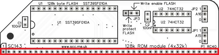
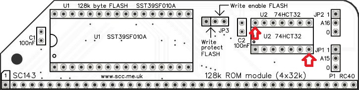
This module includes a 128k byte FLASH memory chip which is divided into four 32k byte banks.
It has been designed primarily as an alternative to the Classic II ROM module which is limited to 8k byte banks. The use of 32k byte banks allows larger firmware to be used.
In theory, the FLASH memory can be written to but this requires special software which is not currently available (as far as I know).
User Guide
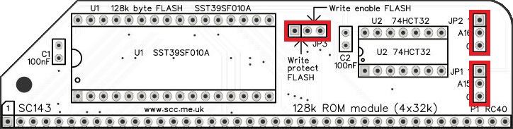
This module includes a 128k byte FLASH memory chip which is divided into four 32k byte banks. The required bank is selected with jumpers JP1 and JP2.
The module will typically be used with jumper shunts fitted in the positions shown below.
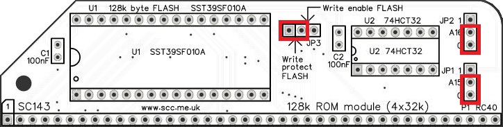
JP1 and JP2 together select which of the four banks are used, as indicated in the table below.
| Bank Number | JP2 (A16) | JP1 (A15) | Typical Contents | |
| 0 | 0 | 0 | SCM S3 v1.0 | |
| 1 | 0 | 1 | Blank | |
| 2 | 1 | 0 | Blank | |
| 3 | 1 | 1 | Blank |
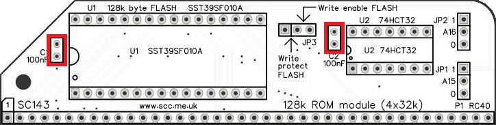
JP3 allows the enabling and disabling of writing to the FLASH memory chip. In normal use it is recommended that the jumper shunt is fitted to protect the FLASH chip from being written, as illustrated above.
In theory, the FLASH chips can be written to with suitable software.
Firmware
The recommended version of the Small Computer Monitor for this board is:
SCM configuration S3
This contains the Small Computer Monitor and BASIC.
Parts List
| Reference | Qty | Component |
| PCB | 1 | SC143, v1.0, PCB |
| C1 and C2 | 2 | Capacitor, ceramic, 100 nF |
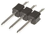
| JP1 to JP3 | 3 | Header, male, 1 row x 3 pin, straight These can be cut from a longer strip |
| Jumper shunts | 3 | Jumper shunts |
| P1 | 1 | Header, male, 1 row x 40 pin, angled |
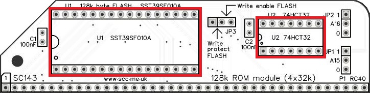
| U1 | 1 | SST39SF010A (128k byte FLASH) |
| U2 | 1 | 74HCT32 (quad 2-input OR) |
| U1 socket | 1 | Socket, DIP, 32-pin |
| U2 socket | 1 | Socket, DIP, 14-pin |
Printed Circuit Board

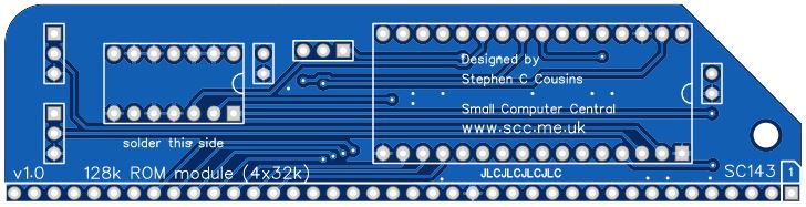
| Links |
| SC143, v1.0, PCB only (Tindie) |
| SC143, v1.0, Complete kit (Tindie) |
| SC143, v1.0, PCB design files (OSHWLab) |
| SC143, v1.0, Gerber files (ZIP) |
Assembly Guide
Experienced builders can just go ahead and populate the board. There shouldn’t be any surprises to catch you out.
Introduction
This guide assumes you are familiar with assembling circuit boards, soldering, and cleaning. If not, it is recommended you read some of the guides on the internet before continuing.
First check you have all the required components.
Before assembling it is worth visually inspecting the circuit board for anything that looks out of place, such as mechanical damage or apparent manufacturing defects.
If you have a multimeter that measures resistance or has a continuity test function, check there is not a short on the power supply tracks. Connect the probes to each terminal of one of the capacitors, such as C1. This should be an open circuit, not a short.
The picture below shows what a completed SC143, ROM module should look like.
Bus connector
Fit and solder the bus header pins P1.
IC sockets
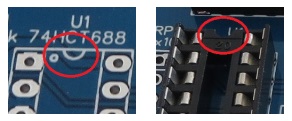
Fit and solder the IC sockets.
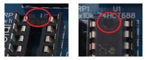
Be sure to fit them with the notch matching the legend on the circuit board, so you do not end up fitting the IC the wrong way around too.
Capacitor 100 nF (0.1 µF)
Fit and solder capacitors, C1 and C2.
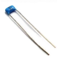
This capacitor can be fitted either way around, as it is not polarity dependent.
The exact value of this component is not critical. The use of very cheap capacitors within the range of about 30 to 200 nF is acceptable.
Headers (straight, single row)
Fit and solder the pin headers JP1, JP2, and JP3.
These header pins may need to be cut from longer strips using wire cutters to cut the plastic.
Inspection
Remove any solder ‘splats’ with a brush, such as an old toothbrush.
Visually inspect the soldering for dry joints and shorts.
Clean the flux off with suitable cleaning materials.
Visually inspect again.
Quick Tests
Repeat the check made earlier for a short. A good place to connect the probes is illustrated below. This should be an open circuit, not a short. If you are using a digital meter set to measure resistance it will likely take a few seconds for the reading to stabilise as there are now capacitors on the power lines. A reading of more than 100k Ω (100000 ohms) is acceptable.
Integrated Circuits
Insert the integrated circuits into their sockets, taking care to insert them the right way round, as illustrated below. Be careful not to bend any legs over.
Getting Started
Jumper shunts will need to be fitted to JP1, JP2, and JP3 before the module can be used. Start with the shunts fitted in the positions shown below. Further details can be found in the User Guide.
Notes
- This design is made in accordance with the “designed for RC2014” labelling scheme.
- RC2014 is a trademark of RFC2795 Ltd.
- This product is designed for hobby use and is not suitable for industrial, commercial or safety-critical applications.
- The product contains small parts and is not suitable for young children.
