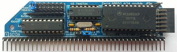
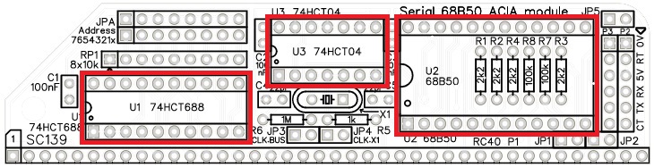
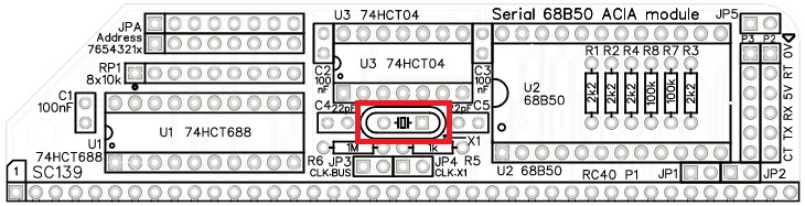
SC139 is a serial 68B50 module designed for the RC2014 bus.
- SC139 – Forum (rc2014)
- SC139 – Forum (retro-comp)
- SC139 – Kit contents sheet (PDF)
- SC139 – Schematic v1.0 (PDF)
Suppliers
| Kits | Website | From | Currency |
| Small Computers Direct | SCDirect | UK | GBP |
| Stephen C Cousins | Tindie | UK | USD |
| PCBs | Website | From | Currency |
| Small Computers Direct | SCDirect | UK | GBP |
| Stephen C Cousins | Tindie | UK | USD |
| Assembled and Tested | Website | From | Currency |
| Not available | |||
| Components | |||
| See parts list |
Description
SC139 is a serial 68B50 module designed for the RC2014 bus.
This serial module has a number of advantages over the standard RC2014 module. It has tight address decoding, flexible address selection, and its own clock. Having its own clock makes it independent of the CPU clock speed, allowing it to be used with faster (or slower) processors. In addition, the serial signals can be isolated from the RC2014 bus, via jumpers, allowing several of these modules to be connected to the same backplane.
The main features of this design are:
- Classic 68B50 serial port
- Tight address decoding
- Address selection via jumpers
- Isolation of serial signals via jumpers
- Compatible with RC2014 bus
- Hardware flow control in both directions
- Low profile RC2014 style design
User Guide
This module provides an asynchronous serial, typically used to connect to a terminal or a modern computer with terminal emulation software.
Serial port
This module provides a 5 volt “TTL” asynchronous serial port, typically set for 115200 baud, 8 data bits, 1 stop bit, no parity.
Both a male and a female connector are provided for maximum flexibility. The optional USB to serial adapter provided with the kit can be plugged directly into the socket or it can be connected with a 6 way Dupont cable fitted to the header pins.

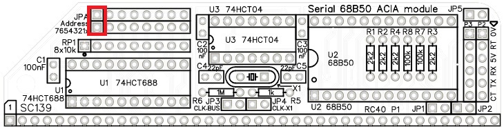
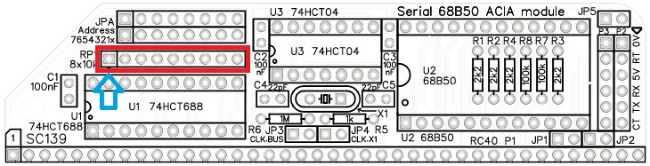
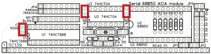
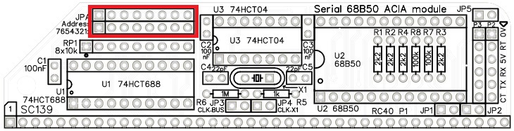
Port address selection
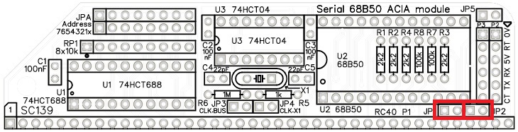
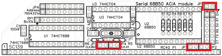
This module occupies 2 input/output port addresses. The base address is set with jumper shunt(s) fitted to the header pins labelled JPA, highlighted below in red. The 2 I/O addresses occupied are BASE ADDRESS and BASE ADDRESS + 1.
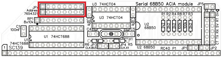
The address selection header is a block of 2 rows of 8 pins. These are the 8 address select jumpers and are labelled with their bit numbers. As the module occupies 2 I/O addresses the least significant bit, bit zero, is not used. All 8 address bits are provided for consistency, but only the most significant 7 bits are needed. You may wish to remove the bit zero pins as a reminder that bit zero is not used. The empty placeholder will act as a reminder.
The module responds to addresses matching the address set with these jumpers. When a jumper shunt is fitted, that bit must be a 1 (high voltage). When the shunt is not fitted, that bit must be a 0 (low voltage).
The default address for an RC2014 is 0x80 (decimal 128, binary 10000000). This is selected by having a single jumper shunts fitted to bit 7, as illustrated below.
The Small Computer Monitor (SCM) supports a seconds 68B50 ACIA serial port at I/O address 0x40 (binary 01000000).
Power
This module is powered from the backplane or from the serial port. If a jumper shunt is fitted to JP5 then power (5 volts) is connected between the serial port and the backplane’s 5 volt supply. This results in the Z80 system being powered from the serial port and/or the serial port being supplied with power from the Z80 system.
You should only have one source of power to the system. If your backplane is powered then you should not also provide power from the serial port.
Typically, the serial port will be connected to a modern computer or terminal through a USB to serial adapter. These adapters are usually powered from the modern computer or terminal, and can provide enough power for a small Z80 system.
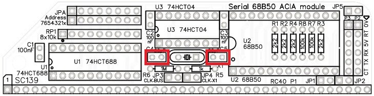
Baud rate clock
The official RC2014 ACIA serial module has its baud rate set by the main bus clock, typically 7.3728 MHz.
This module is more flexible, providing the option of using its on board crystal oscillator. This is selected by fitting a jumper shunt to JP4, as illustrated below.
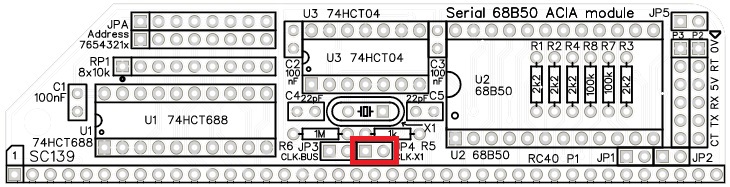
Should you wish to use the main bus clock as the baud rate clock, fit a jumper shunt to JP3 instead of JP4.
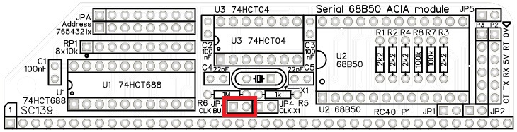
Fitting a jumper shunt to JP3 and another to JP4 enables this module’s on-board oscillator to act as the baud rate clock and also the main bus clock. This could potentially mean you can save a bus slot as you do not need a separate clock module.
You should only have one clock source connected to the main bus clock signal, so do not fit both these jumpers at the same time if you have another clock source in your system.
Serial signals on the bus
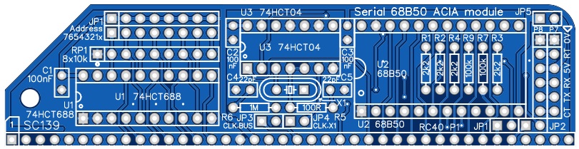
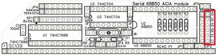
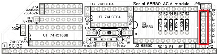
The RC2014 bus allows serial transmit and receive signals to be connected to other modules through the backplane. This module’s transmit and receive signals can be optionally connected to the bus using jumpers JP1 and JP2. Fitting a jumper shunt to JP1 connects the transmit output from this module to the bus pin 35 and JP2 connects the receive input into this module from the bus pin 36.
These jumpers allow more than one serial port module to be fitted to the same backplane. Only one module should have these jumper shunts fitted.
Software
This module is software compatible with the standard RC2014 firmware and software.
Source code for this firmware software is available. This is a good source of example code for this module. One example being the Small Computer Monitor.
Parts List
| Reference | Qty | Component |
| PCB | 1 | SC139, v1.0, PCB |
| C1 to C3 | 3 | Capacitor, ceramic, 100 nF |
| C4 and C5 | 2 | Capacitor, ceramic, 22 pF |
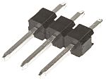
| JP1 plus JP2, and JP3 plus JP4 | 2 | Header, male, 1 x 4 pin, straight |
| JP5 | 1 | Header, male, 1 x 2 pin, straight |
| JPA (Address ) | 1 | Header, male, 2 x 8 pin, angled, or Header, male, 2 x 8 pin, straight |
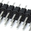
| Jumper shunts | 12 | Jumper shunt |
| P1 | 1 | Header, male, 1 x 40 pin, angled |
| P2 | 1 | Header, female, 1 x 6 pin, angled |
| P3 | 1 | Header, male, 1 x 6 pin, angled |
| R1 to R4 | 2 | Resistor, 2k2, 0.25W |
| R5 | 1 | Resistor, 1k, 0.25W |
| R6 | 1 | Resistor, 1M, 0.25W |
| R7 and R8 | 2 | Resistor, 100k, 0.25W |
| RP1 | 1 | Resistor pack, 8 x 10k, SIL, 9-pin |
| X1 | 1 | Crystal, 7.3728MHz |
| IC socket 20-pin U1 | 1 | 20-pin PDIP socket |
| IC socket 24-pin U2 | 1 | 24-pin PDIP socket |
| IC socket 14-pin U3 | 1 | 14-pin PDIP socket |
| Integrated circuits | ||
| U1 | 1 | 74HCT688 |
| U2 | 1 | 68B50 |
| U3 | 1 | 74HCT04 |
Printed Circuit Board
| Links |
| SC139, v1.0, PCB only (Tindie) |
| SC139, v1.0, Complete kit (Tindie) |
| SC139, v1.0, PCB design files (OSHWLab) |
| SC139, v1.0, Gerber files (ZIP) |
Assembly Guide
Experienced builders can just go ahead and populate the board. There shouldn’t be any surprises to catch you out.
Introduction
This guide assumes you are familiar with assembling circuit boards, soldering, and cleaning. If not, it is recommended you read some of the guides on the internet before continuing.
First check you have all the required components.
Before assembling it is worth visually inspecting the circuit board for anything that looks out of place, such as mechanical damage or apparent manufacturing defects.
If you have a multimeter that measures resistance or has a continuity test function, check there is not a short on the power supply tracks. Connect the probes to each terminal of one of the capacitors, such as C1. This should be an open circuit, not a short.
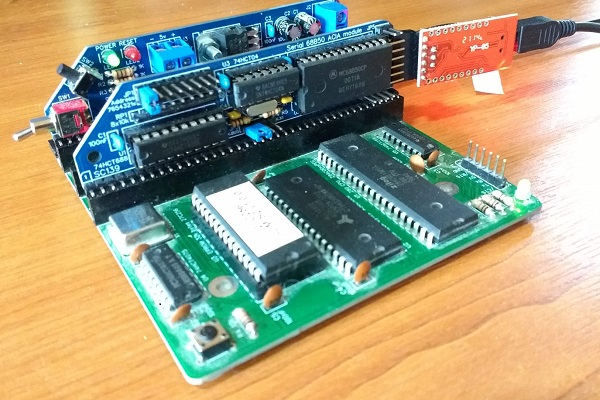
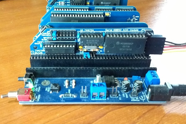
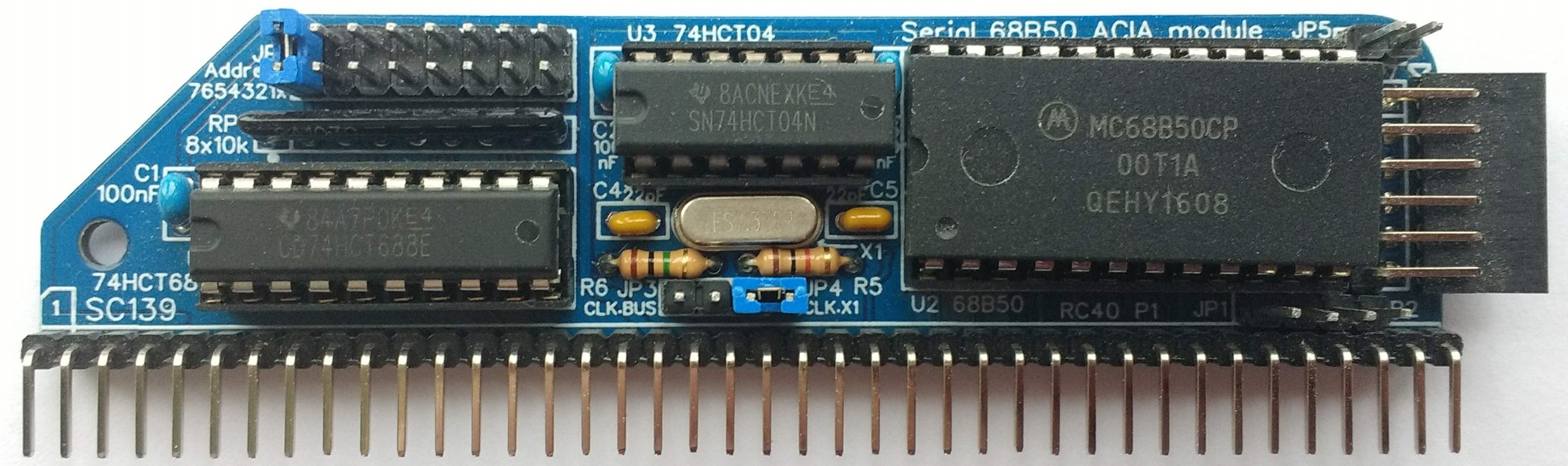
The picture below shows what a completed SC139, serial 68B50 module should look like.
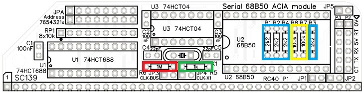
Resistors
Fit and solder the 2k2 resistors R1, R2, R3, and R4 (shown below in blue).

Fit and solder the 1k (1000 ohm) resistor R5 (shown below in green).
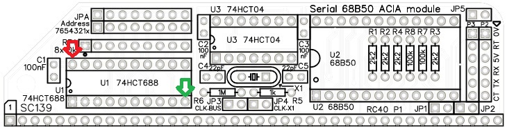
Fit and solder the 1M resistors R6 (shown below in red).

Fit and solder the 100k resistors R7 and R8 (shown below in yellow).
Bus connector
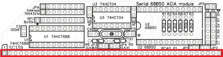
Fit and solder the bus header pins P1.
Serial port socket
Fit and solder the 6-pin female angled header socket P2.

Serial port pins
Fit and solder the 6-pin male angled header pins P3.
Make sure the pins are parallel to the top of the socket P2. If they point down towards the socket you may have trouble fitting a Dupont cable. A good tip is to fit a Dupont cable to the pins when soldering them. Press the Dupont cable housing against the socket, P2, to ensure the pins are parallel.
IC sockets
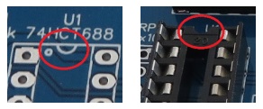
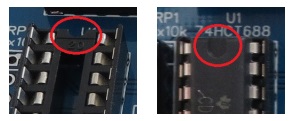
Fit and solder the IC sockets U1 to U3.
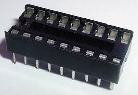
Be sure to fit them with the notch matching the legend on the circuit board, so you do not end up fitting the IC the wrong way around too.
Resistor pack
Fit and solder the 8x10k resistor network RP1 (shown below in red).
The 10k network will be marked 103
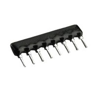
Take care to fit the resistor network the correct way around. Pin 1 is usually marked with a dot. This end is indicated on the PCB and on the illustration below.

Capacitors 100 nF (0.1 µF)
Fit and solder 100nF capacitors C1 to C4.
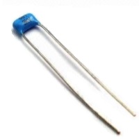
These capacitors can be fitted either way around, as they are not polarity dependent.
The exact value of this component is not critical. The use of very cheap capacitors within the range of about 30 to 200 nF is acceptable.
Capacitors 22 pF
Fit and solder 22pF capacitors C4 and C5.
These capacitors can be fitted either way around, as they are not polarity dependent.
Crystal
Fit and solder the 7.3728 MHz crystal X1.
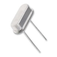
This component can be fitted either way around, as it is not polarity dependent.
Header (double row)
Address selection is via jumper shunts fitted to a double row of header pins. These can either be straight pins or angled pins. Angled pins stick out above the module allowing easy access to the jumper shunts when the module is fitted to a backplane. Straight pins look neater but do not allow the address to be changed when the module is fitted in a backplane with another module immediately in front of it.
Fit and solder the double row straight or angled header pins, JPA.
As only bits 7 to 1, not bit 0, are used to set the address, you may wish to remove the pins for bit zero. See the user guide for an explanation of this.
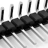
Headers (straight, single row)
Fit and solder the pin headers JP1 to JP5.
These header pins may need to be cut from longer strips using wire cutters to cut the plastic.
Quick Test
Repeat the check made earlier for a short on the power supply tracks. Connect the meter probes to IC U1 pin 20 (shown below in red) and U1 pin 10 (shown in green). This should not be a short circuit. A reading of more than 1 kΩ (1000 ohms) is acceptable.
Inspection
Remove any solder ‘splats’ with a brush, such as an old toothbrush.
Visually inspect the soldering for dry joints and shorts.
Clean the flux off with suitable cleaning materials.
Visually inspect again.
Integrated Circuits
If all the above tests check out okay, insert the integrated circuits into their sockets. Take care to insert them the right way around, as illustrated below. Be careful not to bend any legs over.
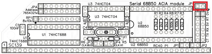
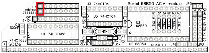
Address select jumpers
Header JPA is a block of header pins with 2 rows of 8 pins. These are the 8 address select jumpers and are labelled with their bit numbers.
The module responds to addresses matching the address set with these jumpers. When a jumper shunt is fitted, that bit must be a 1 (high voltage). When the shunt is not fitted, that bit must be a 0 (low voltage).
If, for example, you wish to set the module to address 128 decimal, which is hexadecimal 80 or binary 10000000, then fit a single jumper shunt to bit 7 (as illustrated below). This is the default address for a 68B50 ACIA.
The least significant address bit (bit 0) does not do anything with this design, but has been included as a place holder for consistency with other modules. You may wish to cut off the pins for bit 0 as a reminder that bit 0 is not used.
You are now ready to give it a try.
Set the module’s address by fitting a jumper shunt in the position illustrated above.
Testing
Connect the module (SC139) to an RC2014 or compatible system that does not have any other serial modules.
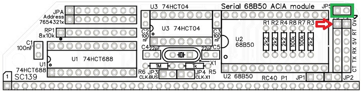
Connect a suitable serial cable to the serial port on this module. Pin 1 of the serial port is indicated below with a red arrow. This is the ground or zero volt pin.
Connect the other end to a computer running suitable terminal software, such as Tera Term. The terminal program should be set for 115200 baud, 8 data bits, 1 stop bit. Flow control is optional but initially it is recommended that flow control is turned off.
If the system is to be powered from the serial port, fit a jumper shunt to JP5 (indicated below in green).
Power up and reset the system. You should get a sign-on message on the terminal.
Notes
- This design is made in accordance with the “designed for RC2014” labelling scheme.
- RC2014 is a trademark of RFC2795 Ltd.
- This product is designed for hobby use and is not suitable for industrial, commercial or safety-critical applications.
- The product contains small parts and is not suitable for young children.
