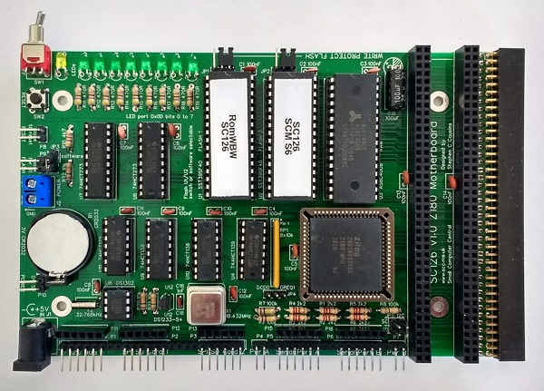
SC126 is a Z180 Motherboard.
- SC126 – Description
- SC126 – Assembly Guide
- SC126 – Circuit Explained
- SC126 – Expansion Cards
- SC126 – Firmware, RomWBW SCZ180_sc126
- SC126 – Firmware, SCM S6
- SC126 – Parts list
- SC126 – Photo Gallery
- SC126 – Printed circuit board
- SC126 – Software, CP/M 2.2
- SC126 – Software, RomWBW
- SC126 – Software, SCM Apps
- SC126 – Support
- SC126 – Troubleshooting
- SC126 – User guide
Downloads
- SC126 – CP/M PutSysPlus (HEX)
- SC126 – Firmware, RomWBW, sc126
- SC126 – Firmware, SCM S6
- SC126 – Kit contents sheet (PDF)
- SC126 – Schematic v1.0 (PDF)
- SC126 – 3D printed parts at thingiverse.com
- SC126 – 3D printed parts at printables.com
Suppliers
| Kits | Website | From | Currency |
| Small Computers Direct | SCDirect | UK | GBP |
| Stephen C Cousins | Tindie | UK | USD |
| Small Computer Central | Lectronz | UK | Euro/USD |
| PCBs | Website | From | Currency |
| Small Computers Direct | SCDirect | UK | GBP |
| Stephen C Cousins | Tindie | UK | USD |
| Small Computer Central | Lectronz | UK | Euro/USD |
| Assembled and Tested | Website | From | Currency |
| Not available | |||
| Components | |||
| See parts list |
Tindie does not collect VAT for EU countries
Lectronz does collect EU VAT for orders up to 150 EUR
Examples
Description
SC126 is a Z180 motherboard and single board computer with expansion sockets compatible with most modules designed for RC2014.

SC126 is my solution to Richard Deane’s design challenge.
Hardware features
- 1 x Z180 processor (33 MHz rated) clocked at 18.432 MHz, with the possibility of software selectable overclocking to 36.864 MHz.
- 1 x 512k byte RAM.
- 2 x 512k byte Flash (ROM), each with its own write enable / write protect jumper. Only one of these is mapped into memory at a time, with selection by jumper, external switch or by software.
- 2 x Serial ports, asynchronous, 5 volt, with software selectable baud rates.
- 2 x SPI ports, primarily for SD card mass storage.
- 1 x Real time clock with battery backup (DS1302).
- 1 x Power On indicator (yellow LED).
- 8 x General purpose software controlled indicators (green LEDs).
- 1 x Bit-bang I2C bus port (master only).
- 1 x Voltage supervisor and reset device (DS1233).
- 5 volt power in by 2.1 mm barrel socket, screw terminal, or pin header.
- 1 x Power ON/OFF toggle switch.
- 1 x Push button reset switch with pin header for external reset switch.
- 2 x BP80 backplane sockets (vertical), compatible with most modules designed for RC2014.
- 1 x BP80 backplane socket (horizontal), which can accept a modular backplane or a module.
- Printed circuit board size 160 mm x 102 mm.
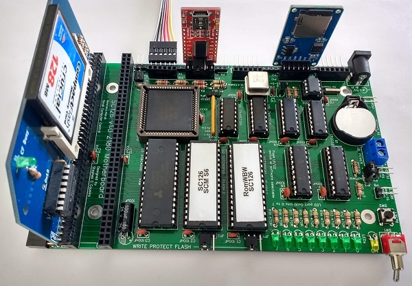
Micro SD Card adapter (shown right) allows connection to the motherboard via Dupont style cable. Alternatively, a female header can be fitted to the motherboard to allow direct connection of the adapter.

Software support
- Small Computer Monitor, configuration S6. This does not offer any support for SD cards, I2C bus, or real time clock.
- RomWBW, configuration RCZ180_sc126. This configuration supports an SD card for mass storage and the real time clock, but not the I2C bus.
RomWBW is the primary OS for SC126, offering CP/M, SD card, real time clock, and CF card support (via RC2014 compatible module).
User Guide
SC126 is a Z180 based motherboard. It can be used on its own as a Single Board Computer or it can be expanded using the built in module sockets. The Expansion sockets allow use of many modules designed for RC2014 and can be further expanded with a modular backplane, such as SC113.
SC126 normally has the Small Computer Monitor (SCM) in one Flash chip and RomWBW in the other.
Documentation for the Small Computer Monitor can be found here.
Documentation for RomWBW can be found here.
A short guide to getting started with RomWBW on SC126 can be found here.

Quick Guide to Jumpers
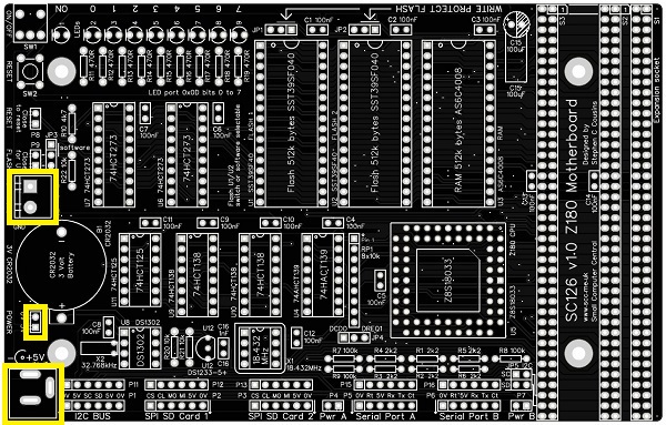
As a quick guide to getting started: Fit jumper shunts in the positions shown below and supply 5 volts to J1 or J2.
And for those who are sensible enough to read User Guides…
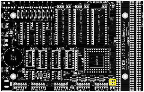
Power
The power required for this board is 5 V D.C. at 100 mA without SD cards or other accessories. With accessories and expansion boards fitted the current requirement could easily rise to 300 mA.
The motherboard can be powered in a number of ways. The illustration below shows three places where 5 volts can be connected. When powered from any of these places the board can be turned on and off with the ON/OFF switch.
The board can also be powered from the serial ports, or even the SPI and I2C ports. Powering from any of these sources does not allow the board to be turn on and off with the ON/OFF switch.
The motherboard is typically connected to a computer or terminal with an FTDI style serial adapter. This can, optionally, also provide power for the motherboard. However, some USB sockets and some FTDI style adapters will not provide adequate power if accessories and expansion cards are connected.
Each serial port, highlighted below in red, can supply power to the system. To connect power from a serial port, fit a jumper shunt in the appropriate location, indicated below in yellow. The left jumper is for port A and the right jumper is for port B.
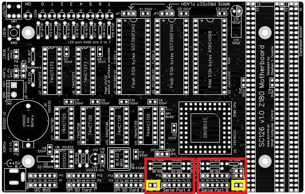
WARNING: You should normally only connect one power source to the system, at any time.
As power can flow either way, these jumpers also enable serial devices to be powered from the motherboard. If such devices are used, fit a jumper shunt in the appropriate position, indicated above in yellow.
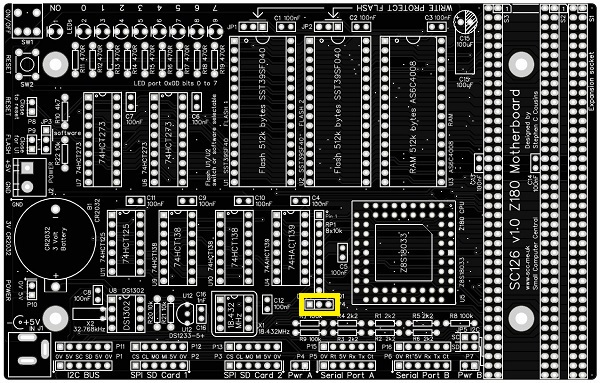
Firmware Selection
The motherboard has two Flash ROM sockets, allowing two different firmware options to be installed at the same time.
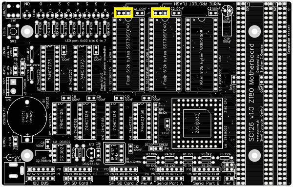
The required firmware is selected with JP3 or P9.

If a jumper shunt or a closed external switch is fitted to P9, then socket U1 is selected. If there is no jumer shunt present or an external switch is open, the socket U2 is selected.
JP3 provides an alternative connection point for a jumper shunt or switch. In addition, it allows a jumper shunt to be fitted in the upper position to allow software control of the socket selection. Socket selection by software is not currently supported.
An external switch connected to P9 carries only a simple D.C. level, so cable length should not normally be a problem.
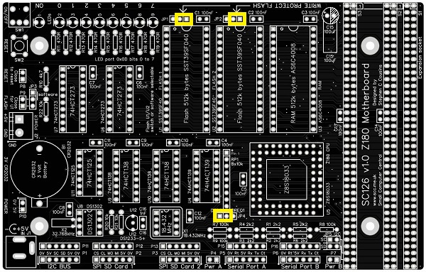
Write Protect Flash
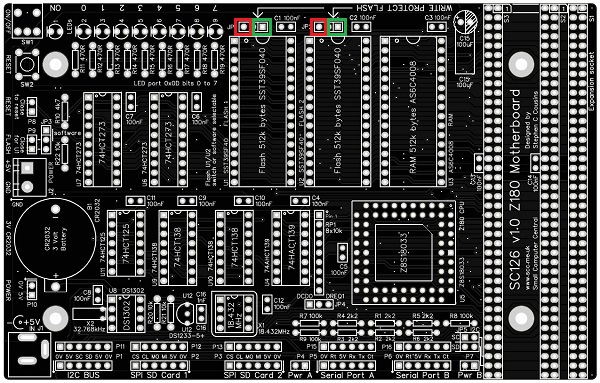
Jumpers, JP1 and JP2, shown below in yellow, enable each Flash chip to be independently write protected. It is unlikely the Flash chip will be corrupted in normal operation, due to the software requirements to write to it. However, for peace of mind you can disable writing with jumper shunts.
Each Flash chip has its own write protection jumper. Fit the shunt in the position shown below in green to disable writing. Alternatively, fit the shunt in the position shown below in red to enable writing.
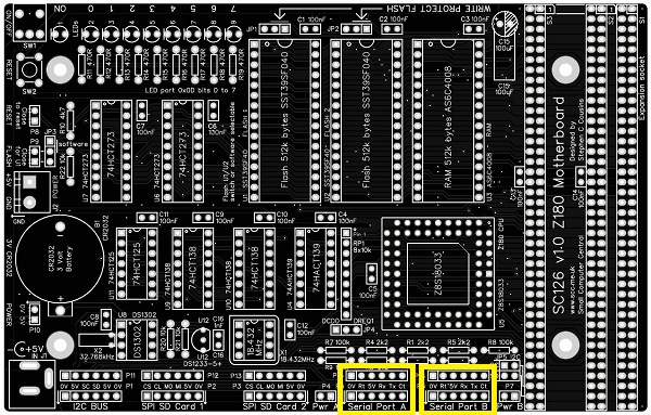
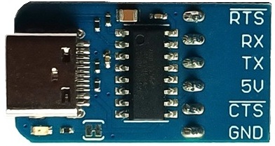
Serial Ports
The motherboard has two asynchronous serial ports, with software selectable baud rate. These are 5 volt FTDI style ports.
The pin-out, below, describes signals with respect to the motherboard, so an output is a signal from the motherboard to a computer or terminal.
| Pin | Function |
| 1 | Ground (GND) |
| 2 | Request To Send (RTS) output |
| 3 | Vcc (5V) |
| 4 | Recieve Data (RxD) input |
| 5 | Transmit Data (TxD) output |
| 6 | Clear To Send (CTS) input (not connected) |
The ground terminal is marked with a small down arrow to help with cable orientation.
A typical FTDI style serial adapter is illustrated to the right.
The default serial ports settings are as follows:
| Setting | SCM | RomWBW |
| Baud rate | 115200 | 115200 (v3.0) 38400 (pre-v3.0) |
| Data bits | 8 | 8 |
| Parity | none | none |
| Stop bits | 1 | 1 |
| Flow control | Hardware (recommended) | Hardware (recommended) |
The default serial port is P5, Serial Port A.
SPI Ports
The motherboard has two SPI ports, primarily for connection to SD card adapters.
The signals are 5 volt levels, with the following pin-out.
| Pin | Function |
| 1 | Chip select (active low) |
| 2 | Clock |
| 3 | Master out, slave in |
| 4 | Master in, slave out |
| 5 | Vcc (5V) |
| 6 | Ground (GND) |
The ground terminal is marked with a small down arrow to help with cable orientation.
A typical micro SD card adapter is illustrated to the right.
This may be fitted directly to the motherboard or by a 6-way cable.
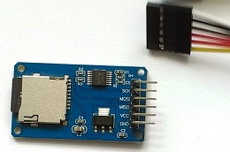
Using the micro SD card adapter illustrated above, only one SPI device may be connected to the motherboard. This is because the adapter does not have a tri-state data output.
The default SD card position is P2, SPI SD Card 1.
Alan Cox designed an adapter board to fix this limitation:
https://hackaday.io/project/167445-spi-fix-for-sc126
I2C Port
The motherboard has a bit-bang I2C bus port. This is a very nice interface for connecting a whole range of slow to modest speed devices, such as digital I/O ports.
This port can only act as an I2C bus master and does not support other bus masters being connected to it.
The signals are 5 volt levels, with the following pin-out.
| Pin | Function |
| 1 | Ground (GND) |
| 2 | Vcc (5v) |
| 3 | Clock (SCL) |
| 4 | Data (SDA) |
| 5 | Vcc (5V) |
| 6 | Ground (GND) |
The I2C signals, SCL and SDA, can be connected to the expansion bus, pins 78 and 79, via two jumpers, JP5 (shown below in yellow).
Expansion Bus Sockets
This is an unofficial variant of the RC2014 Bus. It is essentially an RC2014 Bus with extra pins.
| Row 2 Pin #s | Signal Name | Row 1 Pin # | Signal Name | |
| 41 | Not yet assigned | 1 | A15 | |
| 42 | Not yet assigned | 2 | A14 | |
| 43 | Not yet assigned | 3 | A13 | |
| 44 | Not yet assigned | 4 | A12 | |
| 45 | Not yet assigned | 5 | A11 | |
| 46 | Not yet assigned | 6 | A10 | |
| 47 | Not yet assigned | 7 | A9 | |
| 48 | Not yet assigned | 8 | A8 | |
| 49 | A23 (not used) | 9 | A7 | |
| 50 | A22 (not used) | 10 | A6 | |
| 51 | A21 (not used) | 11 | A5 | |
| 52 | A20 (not used) | 12 | A4 | |
| 53 | A19 | 13 | A3 | |
| 54 | A18 | 14 | A2 | |
| 55 | A17 | 15 | A1 | |
| 56 | A16 | 16 | A0 | |
| 57 | GND | 17 | GND | |
| 58 | 5V | 18 | 5V | |
| 59 | /RFSH | 19 | /M1 | |
| 60 | PAGE (not used) | 20 | /RESET | |
| 61 | CLK2 (not used) | 21 | CLK | |
| 62 | /BUSAK | 22 | /INT | |
| 63 | /HALT | 23 | /MREQ | |
| 64 | /BUSRQ | 24 | /WR | |
| 65 | /WAIT | 25 | /RD | |
| 66 | /NMI | 26 | /IORQ | |
| 67 | D8 (not used) | 27 | D0 | |
| 68 | D9 (not used) | 28 | D1 | |
| 69 | D10 (not used) | 29 | D2 | |
| 70 | D11 (not used) | 30 | D3 | |
| 71 | D12 (not used) | 31 | D4 | |
| 72 | D13 (not used) | 32 | D5 | |
| 73 | D14 (not used) | 33 | D6 | |
| 74 | D15 (not used) | 34 | D7 | |
| 75 | TX2 | 35 | TX | |
| 76 | RX2 | 36 | RX | |
| 77 | USER5 (not used) | 37 | USER1 (not used) | |
| 78 | USER6 (I2C SCL) | 38 | USER2 (not used) | |
| 79 | USER7 (I2C SDA) | 39 | USER3 (not used) | |
| 80 | USER8 (IEI) | 40 | USER4 (IEO) |
The I2C signals, SCL and SDA, can be connected to USER6 (pin 78) and USER7 (pin 79) by fitting jumper shunts to JP5.
Bus pins USER8 and USER4 are used as a Z80 mode 2 interrupt daisy chain, so are not wired straight through link the other signals. Instead USER4 of one socket is connected to USER8 of the next, forming a daisy chain.
DCD0 and DREQ1 Inputs
Header JP4 provides access to the DCD0 input and the DREQ1 input.
With some Z180 processors the DCD0 input must be pulled low (fit jumper shunt) to enable the serial port to receive data. With other Z180 processors this input can be read by suitable software.
Fit a shunt in the DCD0 position to pull the DCD0 input low.
This header should normally have a jumper shunt fitted in the DCD0 position.
Memory Map
The physical memory map is simply 512k byte of Flash ROM at the bottom of memory and 512k bytes of RAM at the top of memory.
The Z180’s memory management unit deals with mapping chunks of this memory into the logical 64k memory map supported by the Z80/Z180 instruction set.
| Address | Function |
| 0x80000 to 0xFFFFF | RAM (512k bytes) |
| 0x00000 to 0x7FFFF | Flash ROM (512k bytes) |
Input / Output Ports
The motherboard’s I/O port addresses are as follows.
| Address | Function |
| 0xC0 to 0xFF | Z180’s internal I/O registers |
| 0x0D | LED output port |
| 0x0C | System I/O port (RTC, SPI and I2C) |
All other I/O addresses are available for use by expansion modules.
The LED port has 8 LEDs which are free for use. These can be written to with simple input and output statements or instructions.
- From BASIC:
- OUT 13, <byte-to-be-output>
- From the Small Computer Monitor
- O D <byte-to-to-output>
- From assembler:
- LD A, <byte-to-be-output>
- OUT ($D), A
The system I/O port can be accessed but care must be taken as the port is shared by several system devices.
Warning: The I2C SDA signal is bi-directional. It has a pull up resistor and can be pulled low by the open collector output on port 0x0C, bit 7. To use I2C SDA as an input the port 0x0C bit 7 output must be set high.
| Port 0x0C | Output function |
| Bit 0 | I2C SCL Connector P1 pin 3 Idle state = high |
| Bit 1 | Optional flash bank select Not normally used for bank select Connector JP3 pin 1 Idle state = not critical |
| Bit 2 | SPI/SD port 1 chip select Connector P2 pin 1 Idle state = high |
| Bit 3 | SPI/SD port 2 chip select Connector P3 pin 1 Idle state = high |
| Bit 4 | Real time clock chip select Not accessible Idle state = high |
| Bit 5 | Real time clock write enable Not accessible Idle state = not critical |
| Bit 6 | Real time clock serial clock Not accessible Idle state = not critical |
| Bit 7 | Real time clock serial data, and I2C SDA serial data output Connector P1 pin 4 Idle state = high |
| Port 0x0C | Input function |
| Bit 0 | Real time clock serial data Not accessible Idle state = not specified |
| Bit 1 | Not used |
| Bit 2 | Not used |
| Bit 3 | Not used |
| Bit 4 | Not used |
| Bit 5 | Not used |
| Bit 6 | Not used |
| Bit 7 | I2C SDA serial data input Connector P1 pin 4 |
To write to the system I/O port use the following.
- From BASIC:
- OUT 12, <byte-to-be-output>
- From the Small Computer Monitor
- O C <byte-to-to-output>
- From assembler:
- LD A, <byte-to-be-output>
- OUT ($C), A
To read from the system I/O port use the following.
- From BASIC:
- X = INP(12)
- From the Small Computer Monitor
- I C <byte-to-to-output>
- From assembler:
- IN A,($C)
Warning: The I2C SDA signal is bi-directional. It has a pull up resistor and can be pulled low by the open collector output on port 0x0C, bit 7. To use I2C SDA as an input the port 0x0C bit 7 output must be set high.
Parts List
| Reference | Qty | Component |
| PCB | 1 | SC126, v1.0, PCB |
| options | 2 | Header, male, 1 row x 40 pin, angled |
| options | 2 | Header, male, 1 row x 40 pin, straight |
| options | 5 | Header, female, 1 row x 6 pin, angled |
| options | 5 | Header, female, 1 row x 6 pin, straight |
| B1 | 1 | Battery holder, CR2032 |
| C1 to C14 | 14 | Capacitor, ceramic, 100 nF |
| C15 | 1 | Capacitor, electrolytic, 100 µF |
| C16 | 1 | Capacitor, ceramic, 1 nF |
| J1 | 1 | Socket, power, barrel, 2.1mm |
| J2 | 1 | Screw terminal, 2 way, 5.08mm pitch |
| JP1 and JP2 | 2 | Header, male, 1 row x 3 pin, angled (cut from longer strip) |
| JP3 and JP4 | 2 | Header, male, 1 row x 3 pin, straight (cut from longer strip) |
| JP5 | 1 | Header, male, 2 row x 2 pin, straight |
| Jumper shunts | 7 | Jumper shunt |
| LED1 | 1 | LED, yellow, 3mm, or LED, orange, 3mm |
| LED2 to LED9 | 8 | LED, green, 3mm |
| P1, 2, 3, 5, 6 See options | 5 | Header, female, 1 row x 6 pin, angled Header, female, 1 row x 6 pin, straight Header, male, 1 row x 6 pin, angled Header, male, 1 row x 6 pin, straight |
| P4, 7, 8, 9, 10 See options | 5 | Header, male, 1 row x 2 pin, angled Header, male, 1 row x 2 pin, straight |
| P11, 12, 13, 15, 16 See options | 5 | Header, female, 1 row x 6 pin, straight Header, male, 1 row x 6 pin, straight |
| P14 | n/a | There is no P14 on SC126 v1.0 |
| R1 to R6 | 6 | Resistor, 2k2, 0.25W |
| R7 to R9 | 3 | Resistor, 100k, 0.25W |
| R10 | 1 | Resistor, 4k7, 0.25W |
| R11 to R19 | 9 | Resistor, 470R, 0.25W |
| R20 to R22 | 3 | Resistor, 10k, 0.25W |
| RP1 | 1 | Resistor pack, 8 x 10k, SIL, 9-pin |
| S1 | 1 | Header, female, 2 row x 40 pin, angled |
| S2 and S3 | 2 | Header, female, 2 row x 40 pin, straight |
| SW1 | 1 | Switch, toggle, sub-miniature, SPDT |
| SW2 | 1 | Switch, tactile button |
| U1 and U2 | 2 | SST39SF040, 512k byte Flash |
| U3 | 1 | AS6C4008, 512k byte SRAM |
| U4 | 1 | 74AHCT139 |
| U5 | 1 | Z8S18020VSG (Z180 CPU), or Z8S18033VSG (Z180 CPU) |
| U6 and U7 | 2 | 74HCT273 |
| U8 | 1 | DS1302+ |
| U9 and U10 | 2 | 74HCT138 |
| U11 | 1 | 74HCT125 |
| U12 | 1 | DS1233-5+ EconoReset |
| X1 | 1 | Oscillator, 18.432 MHz |
| X2 | 1 | Crystal, 32.768 kHz |
| IC socket 8-pin U8, X1 | 2 | 8-pin PDIP socket |
| IC socket 14-pin U11 | 1 | 14-pin PDIP socket |
| IC socket 16-pin U4, 9, 10 | 3 | 16-pin PDIP socket |
| IC socket 20-pin U6 and U7 | 2 | 20-pin PDIP socket |
| IC socket 32-pin U1, 2, 3 | 3 | 32-pin PDIP socket |
| IC socket 68-pin U5 | 1 | 68-pin PLCC socket |
Printed Circuit Board
| Supplier | Website | Ships from |
| Stephen C Cousins | Tindie | UK |
| Small Computer Central | Lectronz | UK |
| pcb4diy | eBay | Germany |
| pcb4diy | pcb4diy.de | Germany |

Notes
- This product is designed for hobby use and is not suitable for industrial, commercial or safety-critical applications.
- The product contains small parts and is not suitable for young children.
