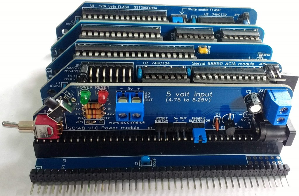
SC148 is a power supply module designed for the RC2014 bus
- SC148 – Support
- SC148 – Kit contents sheet (PDF)
- SC148 – Schematic v1.0 (PDF)
- SC148 – Gerber files (ZIP)
Suppliers
| Kits | Website | From | Currency |
| Small Computers Direct | SCDirect | UK | GBP |
| Stephen C Cousins | Tindie | UK | USD |
| PCBs | Website | From | Currency |
| Small Computers Direct | SCDirect | UK | GBP |
| Stephen C Cousins | Tindie | UK | USD |
| Assembled and Tested | Website | From | Currency |
| Not available | |||
| Components | |||
| See parts list |
Description
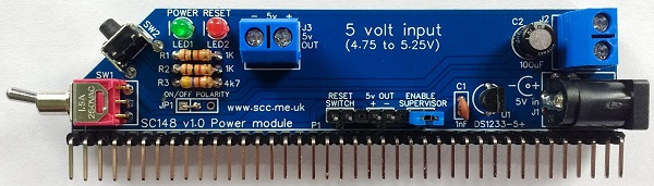
SC148 is a low-profile power supply module designed for the RC2014 bus.
This module supplies power to the RC2014 bus.
The power input must be from a regulated 5 volt D.C. power supply that can provide at least 1 ampere (1000 mA) of current. The 5 volt (nominal) input should be within the range of 4.75 to 5.25 volts.
The module also provides a reset signal to the RC2014 bus. This signal is generated from the onboard reset switch (push button), a reset switch on the backplane, or an external reset switch connected to the onboard pin header. A voltage supervisor and reset device is also included, which provides a reliable power-on reset.
The main features of this design are:
- Voltage input is 5 volts (4.75 to 5.25) at up to 1 amp
- Power input via 2.1mm power jack or screw terminals
- On/Off toggle switch
- Power indicator LED
- 5-volt output via screw terminals and header pins
- Front-facing reset button
- Reset indicator LED
- Voltage supervisor and reset device
User Guide
This module supplies power to the RC2014 bus.
The power input must be from a regulated 5 volt D.C. power supply that can provide at least 1 ampere (1000 mA) of current. The 5-volt (nominal) input should be within the range of 4.75 to 5.25 volts. The switched 5-volt output can be used to power external devices from the onboard screw terminal and pin header.
The module also provides a reset signal to the RC2014 bus. This signal is generated from the onboard reset switch (push button), a reset switch on the backplane, or an external reset switch connected to the onboard pin header. A voltage supervisor and reset device is also included, which provides a reliable power-on reset.
The main features of this design are:
- Voltage input is 5 volts (4.75 to 5.25) at up to 1 amp
- Power input via 2.1mm power jack or screw terminals
- On/Off toggle switch
- Power indicator LED
- 5-volt output via screw terminals and header pins
- Front-facing reset button
- Reset indicator LED
- Voltage supervisor and reset device
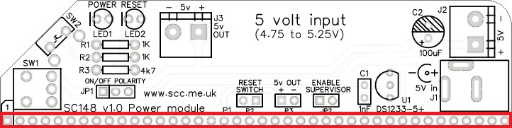
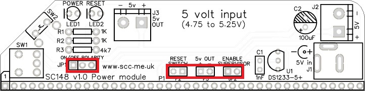
Jumpers
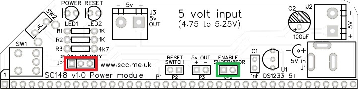
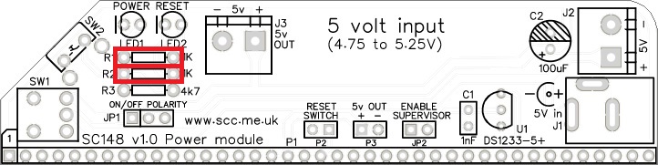
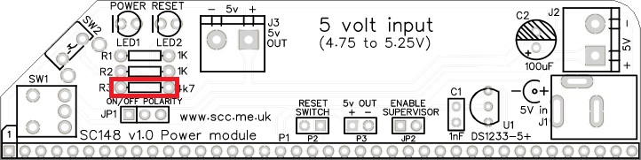
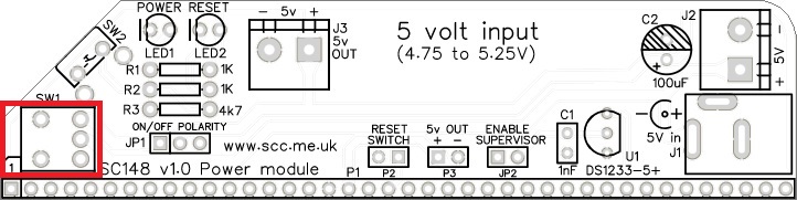
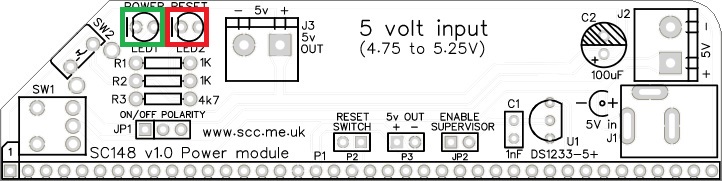
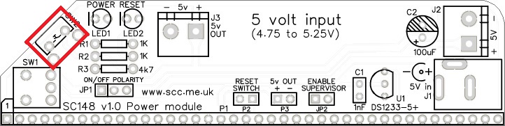
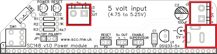
JP1 (shown below in red) can either be constructed using header pins and a jumper shunt, or a soldered link (for greater reliability). If header pins are used then a jumper shunt must be fitted. This jumper shunt or soldered link selects the polarity of the on/off switch, SW1. The convention for ON varies from country to country, with some using UP for ON and others using DOWN for ON. Select your preference with this jumper shunt or soldered link. The left-hand position selects ON = Down, while the right-hand position selected ON = Up.
JP2 (shown below in green) enables the voltage supervisor (U2). This device holds the processor in reset if the voltage is below about 4.7 volts. Fit a jumper shunt here to enable the voltage supervisor, or remove it to disable the supervisor. If the system stays in reset, try disabling the supervisor.
Some other modules also include a voltage supervisor. You should only have one supervisor enabled in your system.
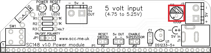
Input supply
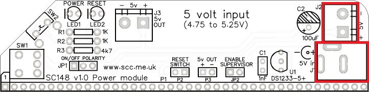
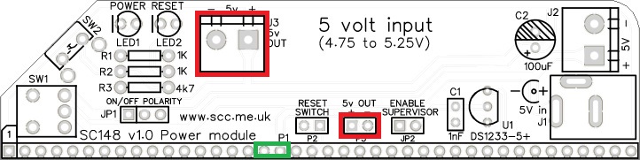
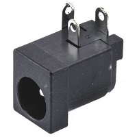
The module is designed for a voltage input of between 4.95 and 5.25 volts D.C. at a maximum of 1 ampere (1000 mA). It is important to connect this supply the correct way around, as indicated by the silkscreen on the circuit board. There are two input connectors, as illustrated below. Either can be used. One is for a power ‘barrel’ style jack plug, which has a 2.1mm centre pin (positive 4.75 to 5.25 volts).
Output supply
In addition to supplying 5 volts to the backplane through the bus pins, illustrated below in green, the module also has connections to power external devices. The two connectors, J3 and P3, provide 5 volts out.
Light Emitting Diodes (LEDs)
LED1 indicates the presence of the 5-volt switched supply. With a suitable supply connected to one of the power inputs and the on/off switch in the ON position, this LED should be ON.
LED2 indicates the bus RESET signal is low. ie. the system is held in reset. This LED should light when the reset button is pressed. If the voltage supervisor is enabled, it should also light for about half a second after switching on.
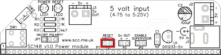
External reset switch
An external reset switch can be connected to the pin header, P2, indicated below. This might be useful if you wish to put your system in a box or position it where the onboard reset button can not easily be reached. A simple momentary action, normally open, switch is all that is required.
Troubleshooting
If the reset LED stays on, the processor will not run as it is in reset. Try disabling the voltage supervisor by removing the jumper shunt on JP2. The voltage supervisor will hold the RESET signal low if the bus supply voltage is below about 4.7 volts. If the problem persists check the reset switch is working. The easiest way to do this is to unplug this module from the backplane and connect a suitable input supply. The reset LED should only be ON when the reset button is pressed.
Parts List
PCB

| Supplier | Website | Ships from |
| Stephen C Cousins | Tindie | UK |
| pcb4diy | eBay | Germany |
| pcb4diy | pcb4diy.de | Germany |
| SC148, v1.0, PCB design files (OSHWLab) |
| SC148, v1.0, Gerber files (ZIP) |
Assembly Guide
Experienced builders can just go ahead and populate the board. There shouldn’t be any surprises to catch you out.
This guide assumes you are familiar with assembling circuit boards, soldering, and cleaning. If not, it is recommended you read some of the guides on the internet before continuing.
First check you have all the required components.
Before assembling it is worth visually inspecting the circuit board for anything that looks out of place, such as mechanical damage or apparent manufacturing defects.
If you have a multimeter that measures resistance or has a continuity test function, check there is not a short on the power supply tracks. Connect the probes to each terminal of one of the connector J3 This should be an open circuit, not a short. Repeat on J2.
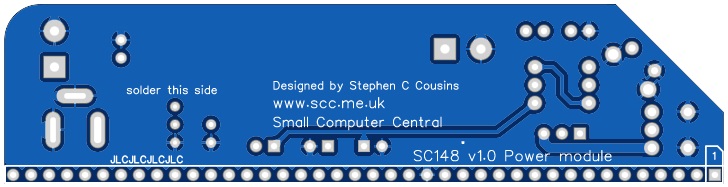
The picture below shows what a completed SC148, power supply module should look like. In the picture below, JP1 is a soldered wire link rather than header pins and a jumper shunt.
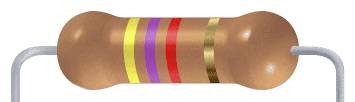
Resistor 1k
Fit and solder the 1k resistors, R1 and R2 (shown below in red).
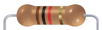
Resistors can be fitted either way around, as they are not polarity dependent.
Resistor 4k7
Fit and solder the 4k7 resistor, R3.
Bus connector
Fit and solder the bus header pins P1.
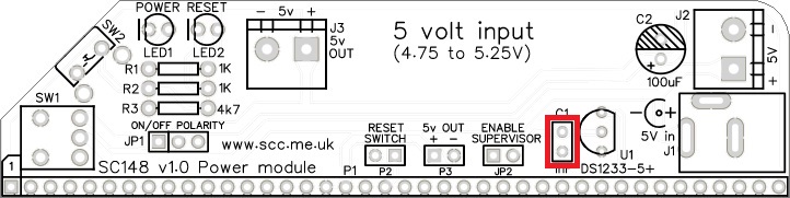
Capacitor 1 nF
Fit and solder capacitor, C1.
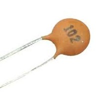
This capacitor can be fitted either way around, as it is not polarity dependent.
The exact value of this component is not critical. The use of very cheap capacitors within the range of about 0.5 to 10 nF is acceptable.
Capacitor 100 µF
Fit and solder capacitors, C1 and C2.
It is important to fit this capacitor the right way around. The negative terminal is indicated with a ‘minus’ sign, as illustrated to the right. The negative terminal also has a shorter lead.
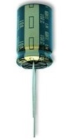
The silkscreen has a plus sign for the positive terminal and a hashed area for the negative terminal
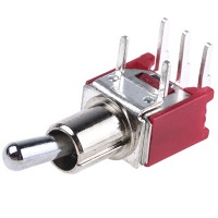
Toggle switch
Fit and solder the toggle switch, SW1.
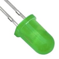
Light Emitting Diode (LED)
Fit and solder the LED1 (green) and LED2 (red).
It is important to fit the LED the correct way around. LEDs usually have a small flat side to indicate the cathode (the negative end). This should be positioned to match the flat side shown on the circuit board (illustrated to the right). Also, the cathode pin on the LED is usually shorter than the other pin (the Anode).


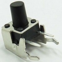
Reset switch
Fit and solder the reset switch, SW2.
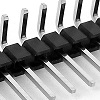
Headers (straight, single row)
Fit and solder the pin headers JP1, JP2, P2, and P3.
JP1 is a 3-pin strip, whilst the others are 2-pin strips.
These header pins may need to be cut from longer strips using wire cutters to cut the plastic.
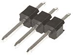
You can make JP2, P2, and P3 from one strip with some pins pulled out of the plastic strip. This makes it easier to keep the three groups in a neat straight row.
Power connectors
Fit and solder the 2.1 mm power jack socket, J1.
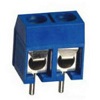
Fit and solder the two screw terminal blocks, J2 and J3.
Ensure the wire entry holes face the edge of the PCB.
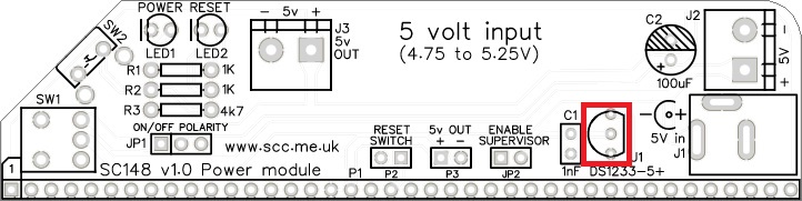
Voltage supervisor and reset
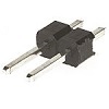
Fit and solder the DS1233 voltage supervisor and reset device, U1.
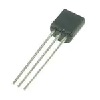
This device must be fitted the correct way around. Match the shape of the device to the legend on the circuit board.
It is necessary to spread the legs of the device to match the hole spacing on the circuit board. Do this gently so as to avoid straining the legs where they enter the plastic casing. Do NOT press the component hard into the board as this will also strain the legs.
Quick Tests
Repeat the check made earlier for a short on the power supply tracks. Connect the meter probes to the terminals of J2. This should be an open circuit, not a short. If you are using a digital meter set to measure resistance it will likely take a few seconds for the reading to stabilise as there are now capacitors on the power lines. A reading of more than 100k Ω (100000 ohms) is acceptable. Repeat with the toggle switch, SW1, in the other position.
Inspection
Remove any solder ‘splats’ with a brush, such as an old toothbrush.
Visually inspect the soldering for dry joints and shorts.
Clean the flux off with suitable cleaning materials.
Visually inspect again.
Getting Started
JP1 can be either a soldered wire link or header pins and a jumper shunt. If header pins are fitted then a jumper shunt will need to be fitted to JP1 before the module can be used. The jumper shunt can be in either position as it just determines the polarity of the on/off switch, SW1, which will be either up for on, or down for on.
A jumper shunt on JP2 is optional, but leave it off for now. This jumper enables the voltage supervisor and reset device, U1.
Connect a suitable regulated 5 volt supply to either J1 or J2. The green power LED should light when the on/off switch, SW1, is in the on position. The red reset LED should be off. Check the voltage at J3 is between 4.75 and 5.25 volts. If it is outside this range, check the voltage at J2 is between 4.75 and 5.25 volts.
Once a good 5-volt supply is known to be available, check the red reset LED comes on when the reset button is pressed and goes off when the reset button is released.
Fit a jumper shunt to JP2. At turn on the red LED should now light for about half a second before turning on. This indicates the power-up reset is working correctly.
Notes
- This design is made in accordance with the “designed for RC2014” labelling scheme.
- RC2014 is a trademark of RFC2795 Ltd.
- This product is designed for hobby use and is not suitable for industrial, commercial, or safety-critical applications.
- The product contains small parts and is not suitable for young children.
