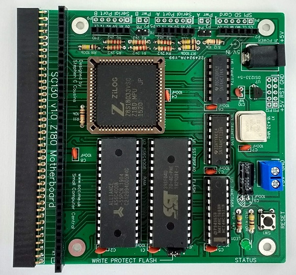
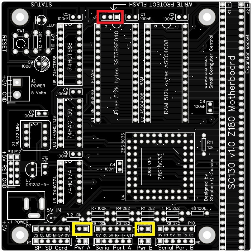
SC130 is an entry-level Z180 Motherboard designed primarily to run RomWBW (and CP/M).
- SC130 – Assembly guide
- SC130 – Firmware, RomWBW_SCZ180_130
- SC130 – Firmware, SCM S6
- SC130 – Photo Gallery
- SC130 – Software, RomWBW
- SC130 – Support
- SC130 – Kit contents sheet (PDF)
- SC130 – Schematic v1.0 (PDF)
- SC130 – SCM-S7.COM (SCM for CP/M)
- SC130 – 3D printed parts at thingiverse.com
Suppliers
| Kits | Website | From | Currency |
| Small Computers Direct | SCDirect | UK | GBP |
| Stephen C Cousins | Tindie | UK | USD |
| Small Computer Central | Lectronz | UK | Euro/USD |
| PCBs | Website | From | Currency |
| Small Computers Direct | SCDirect | UK | GBP |
| Stephen C Cousins | Tindie | UK | USD |
| Small Computer Central | Lectronz | UK | Euro/USD |
| pcb4diy | pcb4diy | Germany | Euro |
| pcb4diy | eBay | Germany | |
| Assembled and Tested | Website | From | Currency |
| Not available | |||
| Components | |||
| See parts list |
Tindie does not collect VAT for EU countries
Lectronz does collect EU VAT for orders up to 150 EUR
Examples
Description
SC130 is a Z180 motherboard and single board computer designed primarily as an entry level platform to run RomWBW (and CP/M).
SC130 includes two 5-volt asynchronous serial ports and an SPI port for connecting a micro SD card adapter. It also has expansion sockets compatible with most modules designed for RC2014.
Hardware features
- 1 x Z180 processor clocked at 18.432 MHz.
- 1 x 512k byte RAM.
- 1 x 512k byte Flash (ROM), typically containing RomWBW.
- 2 x Serial ports, asynchronous, 5-volt, with software selectable baud rates.
- 1 x SPI port, primarily for SD card mass storage.
- 1 x Status LED.
- 1 x Voltage supervisor and reset device (DS1233).
- 5 volt power in by 2.1 mm barrel socket, screw terminal, or pin header.
- 1 x Push button reset switch with pin header for external reset switch.
- 1 x 40-pin vertical backplane socket, compatible with most modules designed for RC2014.
- 1 x 40-pin horizontal backplane socket, which can accept a modular backplane or an RC2014 style module.
- Printed circuit board size 102 mm x 102 mm.
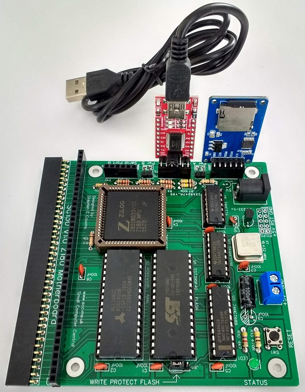
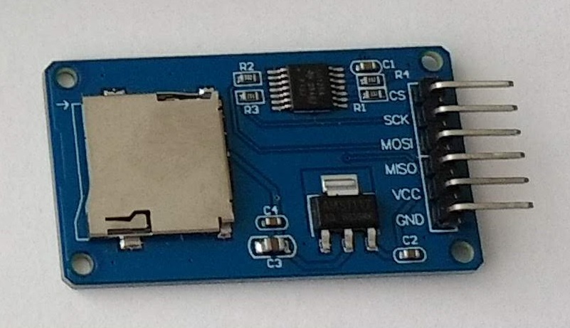
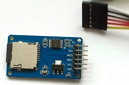
Micro SD Card adapter (shown right) allows a micro SD card to be used for storage of program and data files.
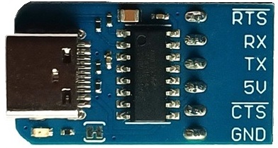
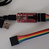
FTDI style 5-volt serial to USB adapter (shown right) allows connection to a computer running a terminal emulation program, such as the Tera Term (free software).
Software support
- RomWBW, configuration SCZ180_sc130. This configuration supports an SD card for mass storage.
RomWBW is the primary OS for SC130, offering CP/M, SD card, and CF card support (via RC2014 compatible module).
User Guide
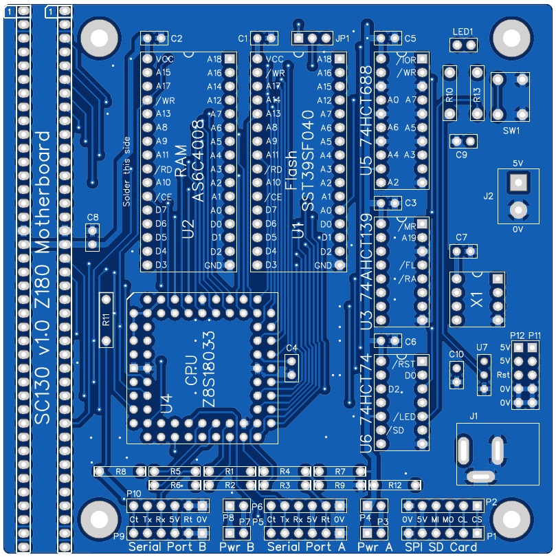
SC130 is a Z180 based motherboard. It can be used on its own as a Single Board Computer or it can be expanded using the built in module sockets. The Expansion sockets allow use of many modules designed for RC2014 and can be further expanded with a modular backplane, such as SC113.
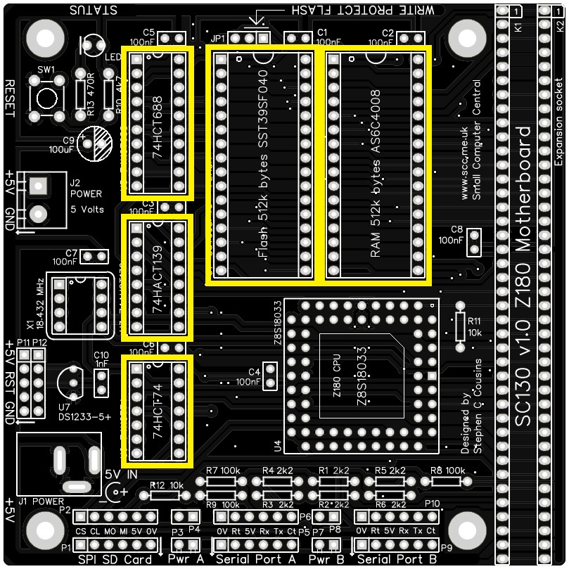
SC130 normally has Flash memory containing RomWBW in socket U1.
Documentation for RomWBW here.
A short guide to getting started with RomWBW on SC130 can be found here.
Quick Guide to Jumpers
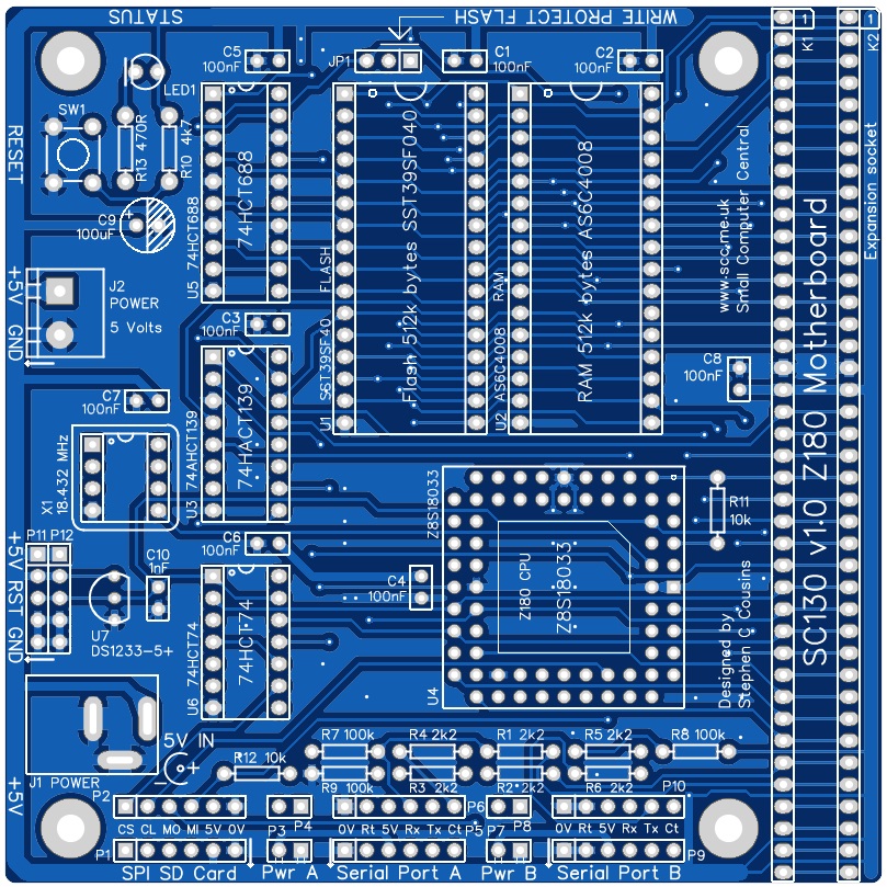
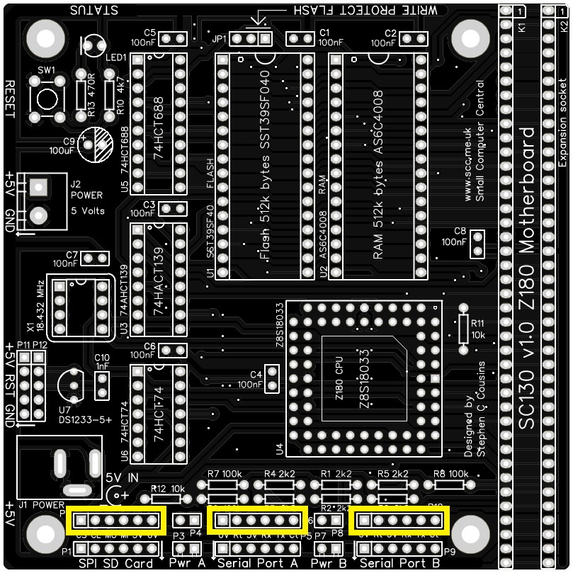
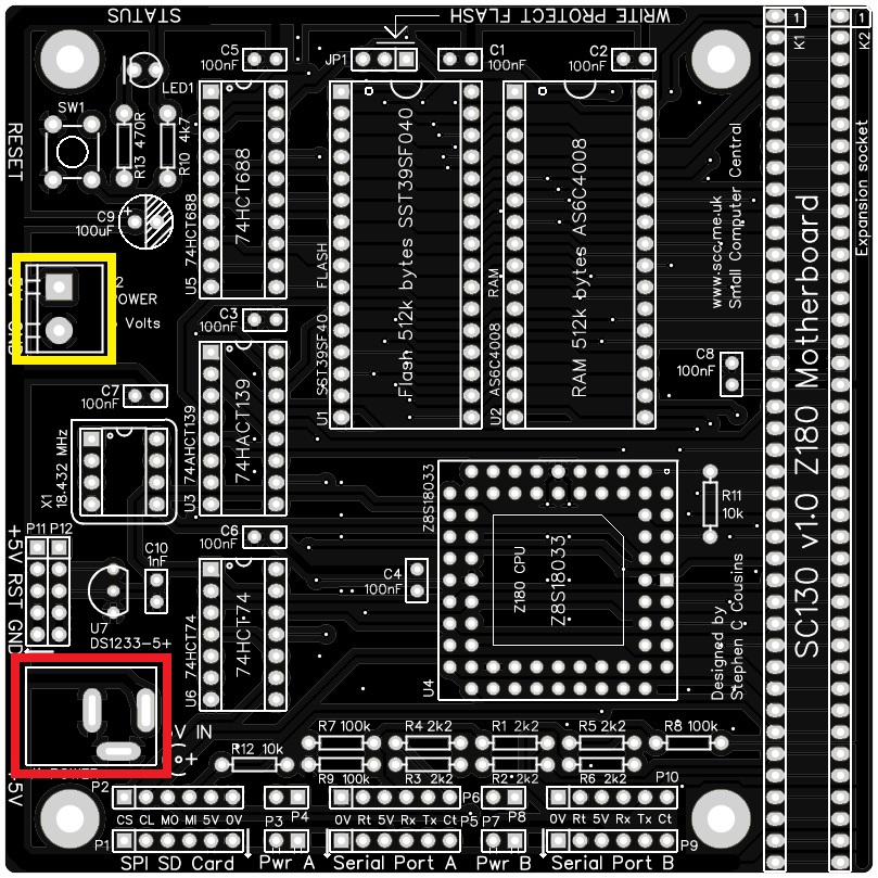
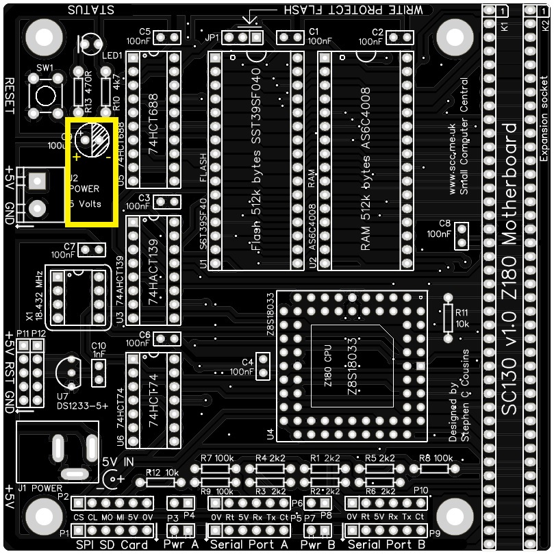
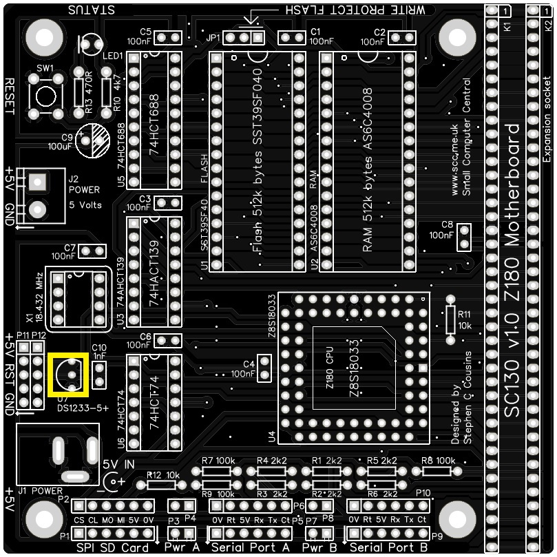
As a quick guide to getting started: Fit a jumper shunt in the position shown below and supply 5 volts to J1 or J2.
And for those who are sensible enough to read User Guides…
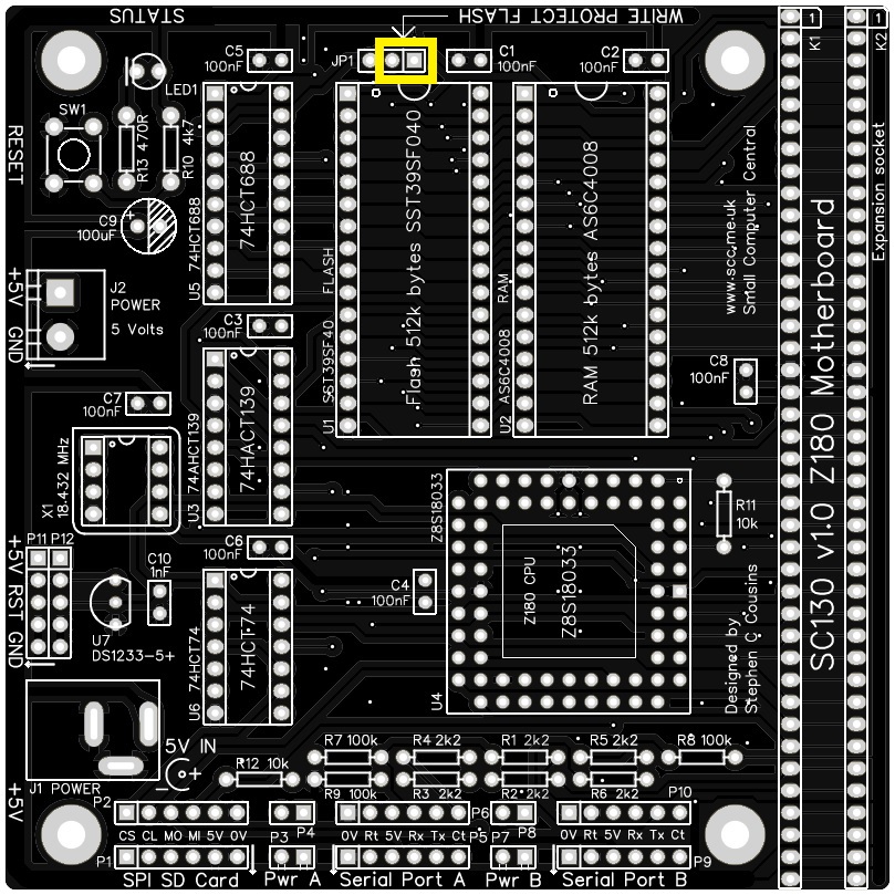
Power
The power required for this board is 5 V D.C. at 100 mA without SD cards or other accessories. With accessories and expansion boards fitted the current requirement could easily rise to 300 mA.
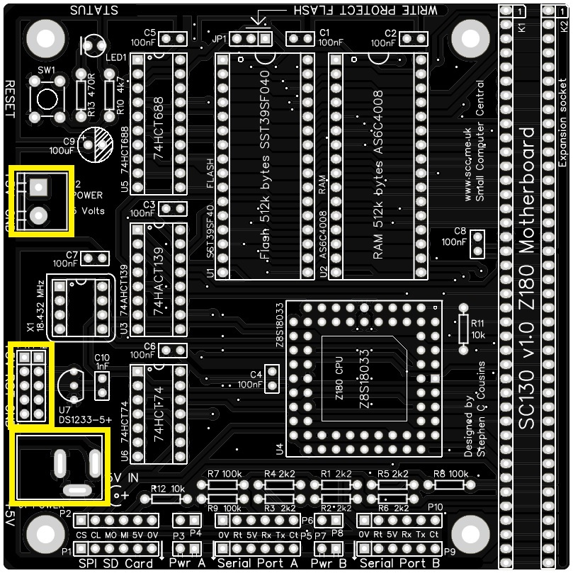
The motherboard can be powered in a number of ways. The illustration below shows three places where 5 volts can be connected.
The board can also be powered from the serial ports or even the SPI port.
The motherboard is typically connected to a computer or terminal with an FTDI style serial adapter. This can, optionally, also provide power for the motherboard. However, some USB sockets and some FTDI style adapters will not provide adequate power if many accessories and expansion cards are connected.
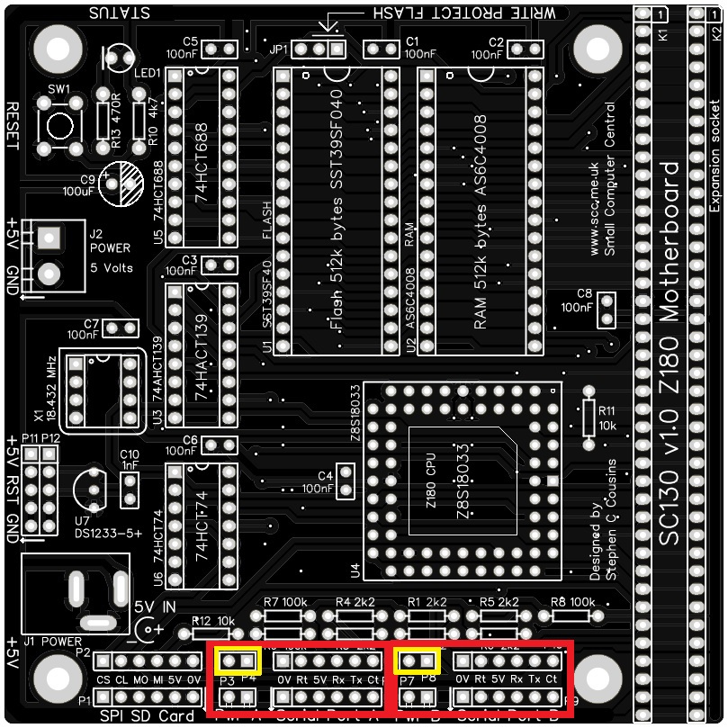
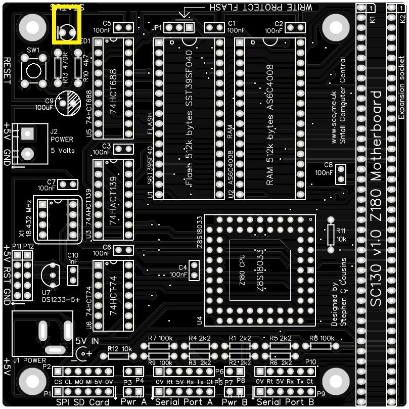
Each serial port, highlighted below in red, can supply power to the system. To connect power from a serial port, fit a jumper shunt in the appropriate location, indicated below in yellow. The left jumper is for port A and the right jumper is for port B.
WARNING: You should normally only connect one power source to the system, at any time.
As power can flow either way, these jumpers also enable serial devices to be powered from the motherboard. If such devices are used, fit a jumper shunt in the appropriate position, indicated above in yellow.
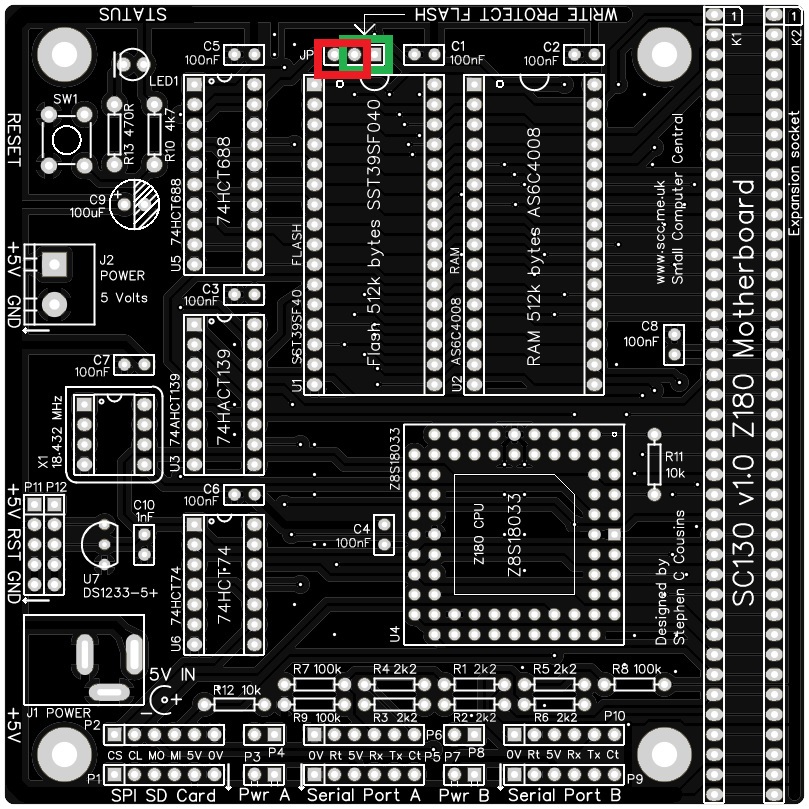
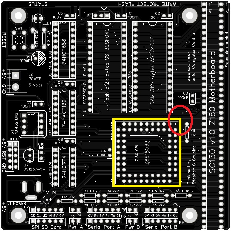
Write Protect Flash
Jumper JP1, shown below in yellow, enables the Flash chip to be write protected. It is unlikely the Flash chip will be corrupted in normal operation due to the software requirements to write to it. However, for peace of mind you can disable writing with jumper shunts.
Fit the shunt in the position shown below in green to disable writing (to write protect the Flash memory). Alternatively, fit the shunt in the position shown below in red to enable writing.
Serial Ports
The motherboard has two asynchronous serial ports, with software selectable baud rate. These are 5 volt FTDI style ports.

The pin-out, below, describes signals with respect to the motherboard, so an output is a signal from the motherboard to a computer or terminal.
| Pin | Function |
| 1 | Ground (GND) |
| 2 | Request To Send (RTS) output |
| 3 | Vcc (5V) |
| 4 | Recieve Data (RxD) input |
| 5 | Transmit Data (TxD) output |
| 6 | Clear To Send (CTS) input (not connected) |
The ground terminal is marked with a small down arrow to help with cable orientation.
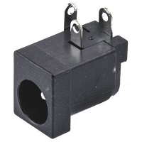
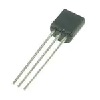
A typical FTDI style serial adapter is illustrated to the right.
The default serial ports settings are as follows:
| Setting | RomWBW |
| Baud rate | 115200 (RomWBW v3.x) 38400 (RomWBW v2.x) |
| Data bits | 8 |
| Parity | none |
| Stop bits | 1 |
| Flow control | Hardware (recommended) |
The default serial port connection is P6, Serial Port A.
SPI Port
The motherboard has an SPI port, primarily for connection of an SD card adapter.

The signals are 5 volt levels, with the following pin-out.
| Pin | Function |
| 1 | Chip select (active low) |
| 2 | Clock |
| 3 | Master out, slave in |
| 4 | Master in, slave out |
| 5 | Vcc (5V) |
| 6 | Ground (GND) |
The ground terminal is marked with a small down arrow to help with cable orientation.
A typical micro SD card adapter is illustrated to the right.
This may be fitted directly to the motherboard or by a 6-way cable.
The default SD card position is connector P2, SPI SD Card.
Expansion Bus Sockets
The expansion connectors are 40-pin RC2014 Bus compatible.
| Pin number | Signal Name |
| 1 | A15 |
| 2 | A14 |
| 3 | A13 |
| 4 | A12 |
| 5 | A11 |
| 6 | A10 |
| 7 | A9 |
| 8 | A8 |
| 9 | A7 |
| 10 | A6 |
| 11 | A5 |
| 12 | A4 |
| 13 | A3 |
| 14 | A2 |
| 15 | A1 |
| 16 | A0 |
| 17 | GND |
| 18 | 5V |
| 19 | /M1 |
| 20 | /RESET |
| 21 | CLK |
| 22 | /INT |
| 23 | /MREQ |
| 24 | /WR |
| 25 | /RD |
| 26 | /IORQ |
| 27 | D0 |
| 28 | D1 |
| 29 | D2 |
| 30 | D3 |
| 31 | D4 |
| 32 | D5 |
| 33 | D6 |
| 34 | D7 |
| 35 | TX |
| 36 | RX |
| 37 | USER1 (not used) |
| 38 | USER2 (not used) |
| 39 | USER3 (not used) |
| 40 | USER4 not used) |
Memory Map
The physical memory map is simply 512k byte of Flash ROM at the bottom of memory and 512k bytes of RAM at the top of memory.
The Z180’s memory management unit deals with mapping chunks of this memory into the logical 64k memory map supported by the Z80/Z180 instruction set.
| Address | Function |
| 0x80000 to 0xFFFFF | RAM (512k bytes) |
| 0x00000 to 0x7FFFF | Flash ROM (512k bytes) |
Input / Output Ports
The motherboard’s I/O port addresses are as follows.
| Address | Function |
| 0xC0 to 0xFF | Z180’s internal I/O registers |
| 0x0E | Status LED port (write only) Bit 0 = LED control (active low) |
| 0x0D | Reserved for LED output port (via expansion module SC129) |
| 0x0C | System I/O port (write only) Bit 2 = SPI select (active low) |
All other I/O addresses are available for use by expansion modules.
The status LED is initially turned on but is otherwise free to use. The LED can be written to with output statements or instructions.
- Turn the status LED off from BASIC:
- OUT 14, 1
- Turn the status LED on from BASIC:
- OUT 14, 0
Note that the LED is turned on by writing a 0 (not a 1). This is because the LED output is active low. This is necessary to allow the LED to be turned on by a hardware reset to indicate power is present. The reset signal clears the output latch to zero, thus zero is the on state.
The optional LED output port has 8 LEDs which are used to display diagnostic information at reset, but are otherwise free for use. These can be written to with simple input and output statements or instructions.
- From BASIC:
- OUT 13, <byte-to-be-output>
- From the Small Computer Monitor
- O D <byte-to-to-output>
- From assembler:
- LD A, <byte-to-be-output>
- OUT ($D), A
Parts List
| Reference | Qty | Component |
| PCB | 1 | SC130, v1.0, PCB |
| C1 to C8 | 8 | Capacitor, ceramic, 100 nF |
| C9 | 1 | Capacitor, electrolytic, 100 µF |
| C10 | 1 | Capacitor, ceramic, 1 nF |
| J1 | 1 | Socket, power, barrel, 2.1mm |
| J2 | 1 | Screw terminal, 2 way, 5.08mm pitch |
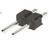
| JP1 | 1 | Header, male, 1 row x 3 pin, straight |
| Jumper shunts | 3 | Jumper shunt |
| K1 | 1 | Header, female, 1 row x 40 pin, straight |
| K2 | 1 | Header, female, 1 row x 40 pin, angled |
| LED1 | 1 | LED, green, 3mm |
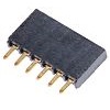
| P2, P6, and P10 | 3 | Header, female, 1 row x 6 pin, straight |
| P4 and P8 | 2 | Header, male, 1 row x 2 pin, straight |
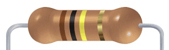
| R1 to R6 | 6 | Resistor, 2k2, 0.25W |
| R7 to R9 | 3 | Resistor, 100k, 0.25W |
| R10 | 1 | Resistor, 4k7, 0.25W |
| R11 and R12 | 2 | Resistor, 10k, 0.25W |
| R13 | 1 | Resistor, 470R, 0.25W |
| SW1 | 1 | Switch, tactile button |
| U1 | 1 | SST39SF040, 512k byte Flash |
| U2 | 1 | AS6C4008, 512k byte SRAM |
| U3 | 1 | 74AHCT139 |
| U4 | 1 | Z8S18020VSG (Z180 CPU), or Z8S18033VSG (Z180 CPU) |
| U5 | 1 | 74HCT688 |
| U6 | 1 | 74HCT74 |
| U7 | 1 | DS1233-5+ EconoReset |
| X1 | 1 | Oscillator, 18.432 MHz |
| IC socket 8-pin X1 | 1 | 8-pin PDIP socket |
| IC socket 14-pin U6 | 1 | 14-pin PDIP socket |
| IC socket 16-pin U3 | 1 | 16-pin PDIP socket |
| IC socket 20-pin U5 | 1 | 20-pin PDIP socket |
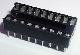
| IC socket 32-pin U1 and U2 | 2 | 32-pin PDIP socket |
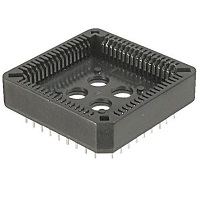
| IC socket 68-pin U4 | 1 | 68-pin PLCC socket |
| Not included in the standard kit | ||
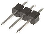
| P1, P5, P9 | 3 | Header, 1 row x 6 pin |
| P11 plus P12 | 1 | Header, 2 row x 5 pin |
Printed Circuit Board
| Supplier | Website | Ships from |
| Stephen C Cousins | Tindie | UK |
| pcb4diy | eBay | Germany |
| pcb4diy | pcb4diy.de | Germany |
Assembly Guide
Experienced builders just go ahead and populate the board. There shouldn’t be any further surprises to catch you out.
This guide assumes you are familiar with assembling circuit boards, soldering, and cleaning. If not, it is recommended you read some of the guides on the internet before continuing.
First check you have all the required components.
Before assembling it is worth visually inspecting the circuit board for anything that looks out of place, such as mechanical damage or apparent manufacturing defects.
If you have a multimeter that measures resistance or has a continuity test function, check there is not a short on the power supply tracks. Connect the probes to each terminal of one of the capacitors, such as C1. This should be an open circuit, not a short.
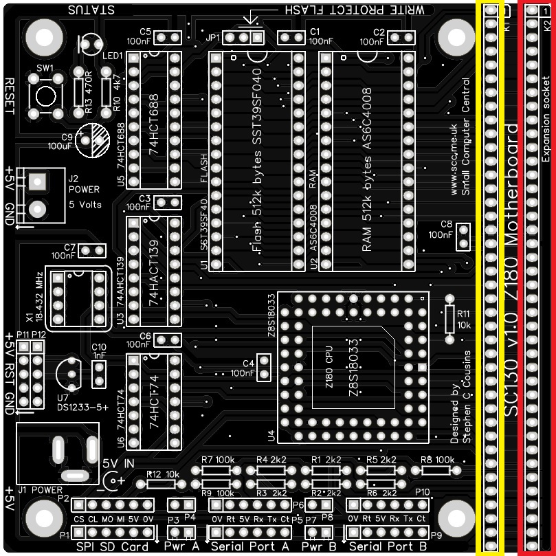
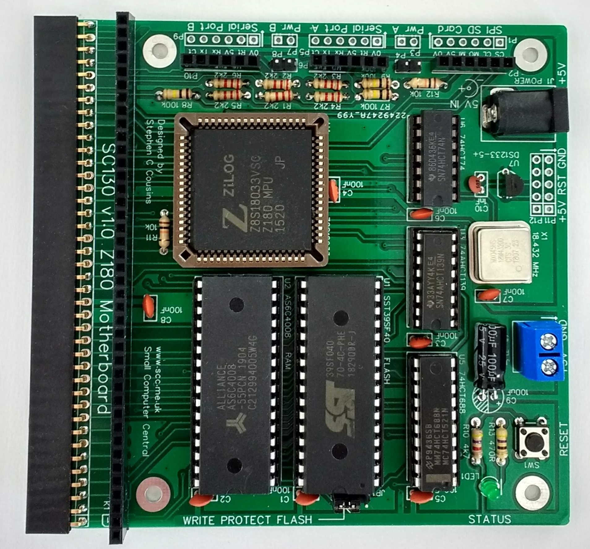
The picture below shows what a completed SC130, Z180 Motherboard should look like.
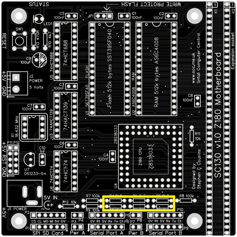
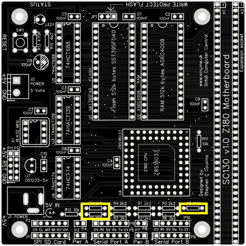
Resistors 2k2
Fit and solder the 2k2 resistors R1 to R6 (shown below in yellow).

These can be fitted either way around, as they are not polarity dependent.
Resistors 100k
Fit and solder the 100k resistors R7 to R9.
Resistor 4k7
Fit and solder the 4k7 resistor R10.
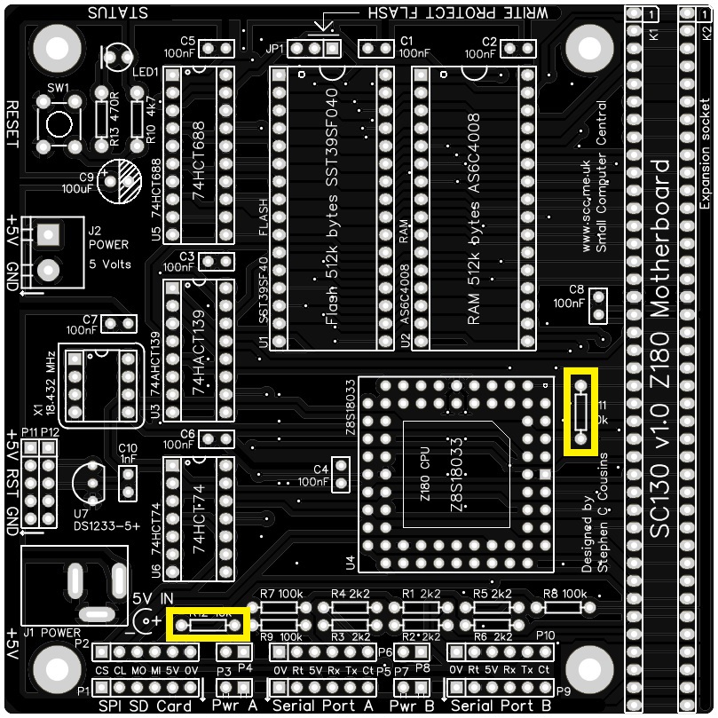
Resistors 10k
Fit and solder the 10k resistors R11 and R12.
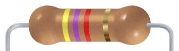
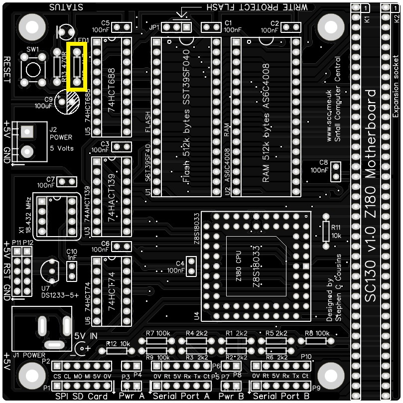
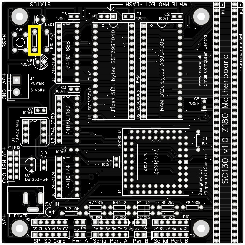
Resistors 470R
Fit and solder the 470R resistors R13.
IC sockets
Fit and solder the IC sockets (shown below in yellow).
Be sure to fit them with the notch matching the legend on the circuit board, so you do not end up fitting the IC the wrong way around too.
PLCC socket
Fit and solder the 68-pin PLCC socket for U4.
This type of socket can be difficult to insert into the PCB holes as there are so many fragile pins, which must be carefully aligned.
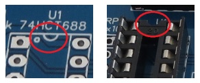
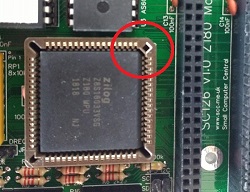
It is vital this socket is fitted the correct way around. The socket has a small chamfer on one corner, as indicated below in red.
Note the position of the chamfered corner, illustrated to the right and also below.

Quick Test
It is now worth repeating the check made earlier for a short on the power supply tracks. Connect the meter probes to each terminal of one of the capacitors, such as C1. This should be an open circuit, not a short.
Capacitor (1 nF)
Fit and solder capacitor C10.

This capacitor can be fitted either way around, as it is not polarity dependent.
The exact value of this component is not critical. The datasheet for the DS1233 specifies a value from 0.5 to 10 nF, thus a very low cost component with a wide tolerance is acceptable.

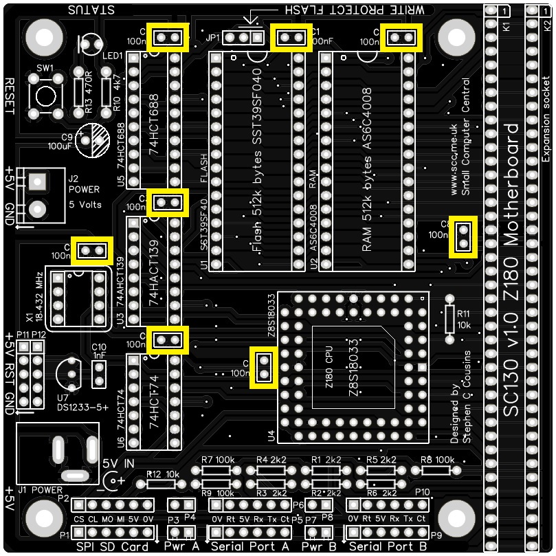
Capacitors 100 nF
Fit and solder capacitors C1 to C8.
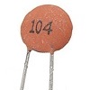
These capacitors can be fitted either way around, as they are not polarity dependent.
The exact value of this component is not critical. The use of very cheap capacitors within the range of about 50 to 100 nF is acceptable.
Bus sockets
Fit and solder the right angled female header, 1 row x 40 pin, K2 (shown below in red).
Fit and solder straight female header, 1 row x 40 pin, K1 (shown below in yellow).
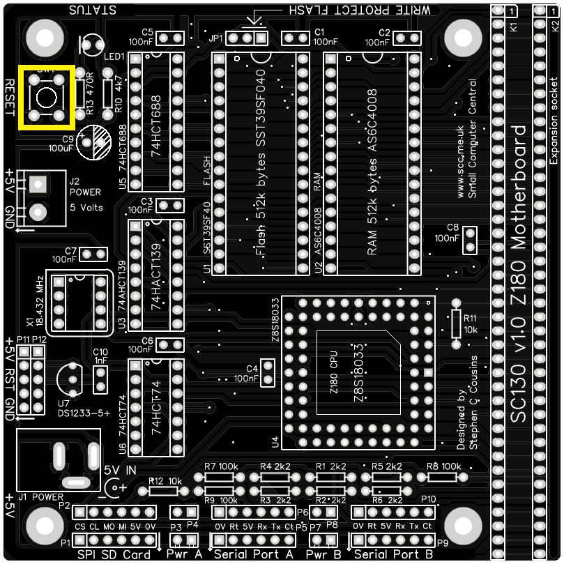
Reset button
Fit and solder push button switch SW1.

Quick Test
Again, repeat the check made earlier for a short on the power supply tracks. Connect the meter probes to IC U6 pin 14 (shown below in red) and U6 pin 7 (shown in green). This should be an open circuit, not a short. If you are using a digital meter set to measure resistance it will likely take a few seconds for the reading to stabilise as there are now capacitors on the power lines. A reading of more than 100 kΩ (100000 ohms) is acceptable.
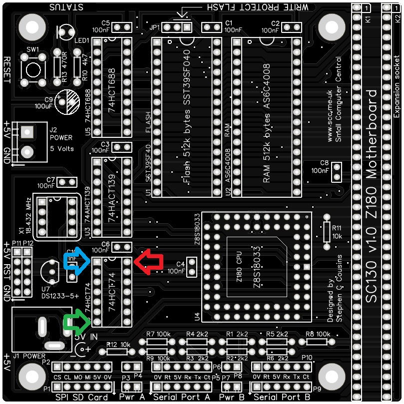
Now measure the resistance between IC U6 pin 14 (red) and U6 pin 1 (blue). This is measuring the pull up resistor R10. It should read 4k7 Ω (4700 ohms) plus or minus 5%.
Also, measure the resistance between IC U6 pin 7 (green) and U6 pin 1 (blue). This is measuring the resistance of the reset switch (SW1). It should currently be open circuit. Again, the reading may take a few seconds to stabilise. A reading of more than 100 kΩ (100000 ohms) is acceptable. Whilst still measuring the resistance, press the reset button. The reading should now be a short circuit. A reading of less than 1 Ω is ideal, but less than 10 Ω is acceptable. The 10 ohm limit has been suggested mainly to allow for measurement accuracy with cheap meters.
Headers (straight)
Fit and solder the pin header JP1 ( 1 row of 3 pins) (shown below in red).
These may need to be cut from longer strips using wire cutters to cut the plastic.
Fit and solder the pin headers P4 and P8 (1 row of 2 pins), (shown below in yellow).
Peripheral ports
Fit and solder 1 row by 5 pin header sockets P2, P6, and P10 (shown below in yellow).
Power connectors
Fit and solder 2.1 mm barrel power socket J1 (shown below in red).
Fit and solder screw terminal J2 (shown below in yellow).

Capacitor (100 µF)
Fit and solder capacitor C9 (shown below in yellow).
It is important to fit this capacitor the right way around. The negative terminal is indicated with a ‘minus’ sign, as illustrated to the right. The negative terminal also has a shorter lead.
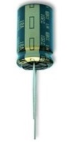
To make the board as low profile as possible, this capacitor can be fitted laying flat, in the position shown below.
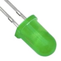
LED
Fit and solder green LED (LED1) in the position shown below.
The LED can either be fitted vertically, with straight leads, or horizontally, by bending the leads.
It is important to fit the LED the correct way around. LEDs usually have a small flat side to indicate the cathode (the negative end). This should be positioned to match the flat side shown on the circuit board (illustrated to the right). Also, the cathode pin on the LED is usually shorter than the other pin (the Anode).

Quick Tests
Repeat the check made earlier for a short on the power supply tracks. Connect the meter probes to IC U6 pin 14 (shown below in red) and U6 pin 7 (shown in green). This should be an open circuit, not a short. If you are using a digital meter set to measure resistance it will likely take a few seconds for the reading to stabilise as there are now capacitors on the power lines. A reading of more than 100k Ω (100000 ohms) is acceptable.
Connect a 5 volt power source to J1 or J2 and perform the following tests. If you do not have a suitable 5 volt power source, connect an FTDI style serial adapter to serial port A and fit a jumper shunt to P4.
- The voltage on the two screw heads of the terminal block J2, should be between 4.75 and 5.25 volts.
- Test the status LED by touching one end of a piece of wire to U6 pin 5 and the other end to U6 pin 7.
- Check the voltage at the middle pin of U7 (RESET) is above 4.5 volts and drops to below 0.5 volts when the reset button is pressed. This should be pulled up by R10.
- Check U1 pin 31 (WR to Flash) is below 0.5 volts but rises to above 4.5 volts when a jumper shunt is fitted to the write protect position of JP1. Without the shunt fitted the signal is floating, so with a digital meter it may not be stable but should be below 0.5 volts.
- Check bus connector pin 22 (INT) is above 4.5 volts. This should be pulled up by resistor network R11.
- Check bus connector pin 36 (RX) is above 4.5 volts. This should be pulled up by R7.
Oscillator (18.432 MHz)
Fit and solder the 18.432 MHz oscillator, X1. Be sure to fit it the correct way around.
Pin 1 of the oscillator is normally indicated by a ‘sharp’ corner, while the other three corners are rounded.
Pin 1 on the circuit board is also indicated by a ‘sharp’ corner, while the other three corners are rounded.


Voltage supervisor and reset
Fit and solder the DS1233 voltage supervisor and reset device U7.
This device must be fitted the correct way around. Match the shape of the device to the legend on the circuit board.
It is necessary to spread the legs of the device to match the hole spacing on the circuit board. Do this gently so as too avoid straining the legs where they enter the plastic casing. DO not press the component hard into the board as this will also strain the legs.
Inspection
Remove any solder ‘splats’ with a brush, such as an old toothbrush.
Visually inspect the soldering for dry joints and shorts.
Clean the flux off with suitable cleaning materials.
Visually inspect again.
Quick Test
Connect a 5 volt supply or the FTDI cable (as described earlier). Check the voltage at U6 pin 1 (RESET). It should be above 4.5 volts. Check it drops below 0.5 volts when the reset button is pressed and returns to above 4.5 volts within one second of the reset button being released.
If you have a variable voltage supply you can check the voltage supervisor (U12) pulls the reset line low when the voltage drops below about 4.6 volts. This is not an exact voltage level, there is a significant tolerance, but it should trip between 4.5 and 4.75 volts.
Integrated Circuits
If all the above tests check out okay, disconnect the power and insert the integrated circuits into their sockets.
Fit the Z180 CPU into its socket as illustrated to the right. This must be fitted the correct way around. The socket and IC both have a small chamfer in the position indicated.
Take care to insert the Z180 CPU level. Avoid pressing one side in while the other side is still raised. If you need to remove the IC it is worth getting a special tool which hooks under opposite corners of component so that it can be lifted out evenly.
Fit a jumper shunt in the positions shown below.
Initial Testing
Connect the 5 volt supply and turn on. The status LED should light for a fraction of a second, then blink off for about half a second, then light again. This indicates the self test has passed.
If the self test completes correctly, power down and connect serial port A to a computer running terminal software.
An FTDI style serial adapter and cable is typically used to connect to the computer, as illustrated to the right.
The terminal software should be set for 115200 baud, 8 data bits, no parity, 1 stop bit, and no flow control. Power up and you should see the startup message.
Note: With RomWBW v2.x the baud rate is 38400 baud.
Given that the self test passed, a failure to display the start up message is most likely to be directly related to the serial port electronics or the serial adapter cable. Check for activity at the serial port connector and around the 2k2 resistors.
If all is well set the terminal software to use hardware flow control and check you still see the startup message. It is recommended that hardware flow control be used where possible.
Troubleshooting
This guide is for anyone who has an SC130 that does not work.
Unless otherwise specified the following tests are performed with a low cost digital multimeter.

Results, below, are shown in a table which has a column for each of the following:
- Test – Description of the test
- My unit – Results on my SC130
- Min. – Minimum acceptable value
- Max. – Maximum acceptable value
Perform each check in the order described and, if possible, resolve any problem found before moving on to the next check.
Visual Inspection
From my experience I think the most likely problem will be an assembly issue. These can often be found with visual inspection, so take your time and carefully do the following:
- Check components are in the correct locations and are fitted the correct way around.
- Look for any IC leg that is bent under the chip and not making contact with the socket.
- With a magnifying glass (or similar) inspect all solder joints looking for any that may have a short to other components or where the solder has not flowed nicely onto the pad and component lead.
Never underestimate the importance of visual inspection.
Jumpers
The following tests assume a jumper shunt is fitted in the position shown below.
The write protection jumper (JP1) should have a shunt fitted in the ‘Write protect flash’ positions.
Power supply
With the board not connected to a power source and nothing else connected to the motherboard, use a multimeter to check there is not a short on the power lines. The meter reading may take a while to settle due to capacitance.
| Test | My unit | Min. | Max. |
| Power supply resistance measured at screw terminal (J2) | > 1 Mꭥ | 10 kꭥ | n/a |
A value below the minimum would likely indicate a short circuit, such as a solder splash. A less likely cause would be a faulty component, such as a decoupling capacitor.
The following tests are carried out with a 5 volt power source connected to either the screw terminals (J2), the barrel socket (J1), or one of the serial port headers (P2 or P6). When using the serial port power source, fit a jumper shunt to P4 (serial port A) or P8 (serial port B).
| Test | My unit | Min. | Max. |
| Power supply voltage measured at screw terminal (J2) | 4.93 V | 4.75 V | 5.25 V |
If you have a means of measuring the power supply current, do so now.
| Test | My unit | Min. | Max. |
| Power supply current running RomWBW | 40 mA | 30 mA | 60 mA |
A value below the minimum suggested value might indicate a broken track such that power is not reaching all of the components. A value around the minimum suggested value could be caused by the oscillator not running so that there is very little activity on the board, and thus low current consumption.
A value above the maximum might be caused by a faulty component, a short circuit somewhere, or perhaps an IC inserted the wrong way around.
Reset
The processor won’t run if the reset signal is low.
| Test | My unit | Min. | Max. |
| Voltage from U6 pin 7 (GND) to U6 pin 1 (/RESET) Reset button not pressed | 4.9 V | 4.0 V | 5.25 V |
| Voltage from U6 pin 7 (GND) to U6 pin 1 (/RESET) Reset button pressed | 0.0 V | 0.0 V | 0.5 V |
Check this voltage drops to less than 0.5 volts when the reset button is pressed. When the reset button is released, the reset signal should go high (> 4.0 V) within about 1 second.
If the reset signal stays low, there could be a problem around U7 (the voltage supervisor and reset chip), C10, or the reset button (SW1).
Power LED does not light up
Skip this section if the status LED (LED1) lights when power is applied, then blinks off for about half a second, then turns on and stays on.
If the LED lights but does not then blink off and on as described above, it is likely that there is a fault around IC U6 or the processor is not running the firmware correctly when it comes out of reset. If you can’t see a problem around U6 then skip the rest of this section.
Press and hold the reset button. If the LED lights but did not light at power up, then go back and check the reset signal again. If the LED does no light then continue with these tests.
| Test | My unit | Min. | Max. |
| Power supply voltage at IC U6, pins 7 and 14 | 4.93 V | 4.75 V | 5.25 V |
If the voltage is missing at IC U6 then check bad solder joints on the power tracks.
| Test | My unit | Min. | Max. |
| Voltage from screw terminal (J2) GND to resistor R13 (near power LED) Test end of resistor furthest away from LEDs | 0.17 V | 0.0 V | 0.5 V |
If this voltage is above the maximum, then U6 pin 5 is not pulling the signal low. At reset the two D-type flip-flops in U6 should be cleared. A cleared output on pin 5 should be low. As we have already checked the reset signal it is possible that IC U6 is faulty.
| Test | My unit | Min. | Max. |
| Voltage from screw terminal (J2) GND to resistor R13 (near power LED) Test end of resistor nearest the LEDs | 2.99 V | 2.5 V | 3.5 V |
If the voltage is not within the specified range, it is likely the LED is fitted the wrong way around or is faulty. Also, check solder joints and tracks around R13 and LED1.
Clock
The processor won’t run without a clock signal.
| Test | My unit | Min. | Max. |
| Voltage from any ground point to X1 pin 5 (CLKX) | 2.48 V | 2.0 V | 3.0 V |
If the voltage is not within the specified range, it is likely the oscillator is faulty, power is not reaching the oscillator, there is a bad joint around X1 or there is a short on the CLKX line.
Self-test LED sequence
Following a reset, the status LED should light for a fraction of a second, then blink off for about half a second, then light again. This indicates the self test has passed.
RomWBW uses an output port driving 8 LEDs to display the results of self-test diagnostics following a reset. A suitable port is SC129 set to address 0x0D.
RomWBW lights the LEDs in sequence, such that a successful test results in all 8 LEDs being turned on. This is described in detail here.
More power tests
Check the 5 volt supply reaches the following places by measuring the voltage at the points indicated.
| Test | My unit | Min. | Max. |
| IC U1 between pins 16 and 32 | 4.94 V | 4.75 V | 5.25 V |
| IC U2 between pins 16 and 32 | 4.94 V | 4.75 V | 5.25 V |
| IC U3 between pins 8 and 16 | 4.94 V | 4.75V | 5.25 V |
| IC U4 between pins 36 and 34 This can be tricky so skip this measurement if you are concerned | 4.94 V | 4.75 V | 5.25 V |
| IC U5 between pins 10 and 20 | 4.94 V | 4.75 V | 5.25 V |
| IC U6 between pins 7 and 14 | 4.94 V | 4.75 V | 5.25 V |
Bus signals
Check the voltage on the bus signals indicated in the tables below.
The voltages will depend on what the processor is doing, so on a faulty system they may not follow the pattern indicated by my test results. Also, a different version of the firmware will result in a different pattern of voltages.
If any of these signals are say less than 0.1 bolts or within 0.1 volts of the power supply voltage, it is likely there is a short between the signal and ground or the signal and 5 volts.
If any of these signals is outside the suggested range but not within 0.1 volts of ground or the power supply, then there could be a short between this signal and another signal, or it could just be the processor is running a tight loop and keeping the signal in one state nearly all the time.
If you have an oscilloscope, you will get a better idea of what is going on by looking at the signals at these locations, looking for floating signals or poorly shaped signals.
| Test | My unit | Min. | Max. |
| IC U2 between pins 16 and 13 (D0) | 2.7 V | 1.2 V | 3.5 V |
| IC U2 between pins 16 and 14 (D1) | 2.4 V | 1.2 V | 3.5 V |
| IC U2 between pins 16 and 15 (D2) | 2.6 V | 1.2 V | 3.5 V |
| IC U2 between pins 16 and 17 (D3) | 2.4 V | 1.2 V | 3.5 V |
| IC U2 between pins 16 and 18 (D4) | 1.9 V | 1.2 V | 3.5 V |
| IC U2 between pins 16 and 19 (D5) | 2.4 V | 1.2 V | 3.5 V |
| IC U2 between pins 16 and 20 (D6) | 2.3 V | 1.2 V | 3.5 V |
| IC U2 between pins 16 and 21 (D7) | 2.5 V | 1.2 V | 3.5 V |
| Test | My unit | Min. | Max. |
| IC U2 between pins 16 and 12 (A0) | 2.5 V | 1.2 V | 3.5 V |
| IC U2 between pins 16 and 11 (A1) | 2.4 V | 1.2 V | 3.5 V |
| IC U2 between pins 16 and 10 (A2) | 2.5 V | 1.2 V | 3.5 V |
| IC U2 between pins 16 and 9 (A3) | 2.8 V | 1.2 V | 3.5 V |
| IC U2 between pins 16 and 8 (A4) | 3.2 V | 1.2 V | 3.5 V |
| IC U2 between pins 16 and 7 (A5) | 3.2 V | 1.2 V | 3.5 V |
| IC U2 between pins 16 and 6 (A6) | 2.5 V | 1.2 V | 3.5 V |
| IC U2 between pins 16 and 5 (A7) | 2.0 V | 1.2 V | 3.5 V |
| Test | My unit | Min. | Max. |
| IC U2 between pins 16 and 27 (A8) | 2.1 V | 1.2 V | 3.5 V |
| IC U2 between pins 16 and 26 (A9) | 3.6 V | 1.2 V | 3.5 V |
| IC U2 between pins 16 and 23 (A10) | 3.3 V | 1.2 V | 3.5 V |
| IC U2 between pins 16 and 25 (A11) | 3.4 V | 1.2 V | 3.5 V |
| IC U2 between pins 16 and 4 (A12) | 1.5 V | 1.2 V | 3.5 V |
| IC U2 between pins 16 and 28 (A13) | 1.4 V | 1.2 V | 3.5 V |
| IC U2 between pins 16 and 3 (A14) | 1.5 V | 1.2 V | 3.5 V |
| IC U2 between pins 16 and 31 (A15) | 4.9 V | 1.2 V | 3.5 V |
| Test | My unit | Min. | Max. |
| IC U2 between pins 16 and 24 (RD) | 2.3 V | 1.2 V | 3.5 V |
| IC U2 between pins 16 and 29 (/WR) | 4.6 V | 4.0 V | 5.25 V |
| IC U2 between pins 16 and 22 (CE) | 1.9 V | 1.2 V | 3.5 V |
If any of these signals looks wrong, try measuring the voltage when you press and release the reset button.
If the voltage levels do not appear to change during that first second, it is likely the processor is not running the firmware code in the expected way.
Circuit Explained
The SC130, Z180 SBC/motherboard includes the following:
- Z180 CPU running at 18.432 MHz
- One 512k byte static RAM chip
- One 512k byte Flash ROM chips
- Two 5 volt FTDI style asynchronous serial ports
- One 5 volt SPI / SD Card ports
- Clock oscillator (18.432 MHz)
- Power supply supervisor and a reset circuit
- Two expansion sockets
- Power input (5 volt, typically 100 mA)
C1 to C8
These capacitors provide power supply decoupling (or bypass). The fast switching in digital circuits creates spikes on the power supply lines which are suppressed with decoupling capacitors placed at key points on the circuit board.
The exact value of this component is not critical. The use of very cheap capacitors within the range of about 50 to 100 nF is acceptable.
C9
This capacitor provides additional support for transient current demands.
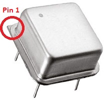
C10
This capacitor is required by the Voltage Supervisor and Reset device (DS1233-5+, U7) when an external reset switch and pull-up resistor are connected to the reset line. See DS1233-5+ datasheet for more details.
The exact value of this component is not critical. The datasheet for the DS1233 specifies a value from 0.5 to 10 nF, thus a very low cost component with a wide tolerance is acceptable.
J1
Barrel style, 5 volt power input socket.
J2
Screw terminal, 5 volt power input.
JP1
Jumper 1 allows Flash chip U1’s write enable input to be connected to either Vcc (5 volts) or the CPU’s write output (/WR).
When the Flash chip’s write enable input is connected to Vcc, the Flash chip will never get a write enable signal and thus the memory is protected against being changed. When connected to the CPU’s write output, it is possible to write to the Flash chip.
Writing to the Flash chip is unlikely to happen by accident due to the software requirements. However, for peace of mind it is generally best to disable writing with this jumper.
K1
This is a 40-pin RC2014 bus socket, mounted vertically to allow expansion modules to be fitted.
K2
This is an 40-pin RC2014 bus socket, mounted horizontally to allow a module backplane extension board, such as SC113, to be fitted. It can also be used to connect an expansion module horizontally.
LED1
This LED is used to indicate the presence of the 5 volt supply and also other status information. At reset the LED is turned on by hardware but after that it is software controlled.
P1 and P2
These connectors give access to the 5 volt SPI port. This port uses the Z180’s hardware clocked serial I/O for high speed interfacing.
| Pin | Function |
| 1 | Chip select (active low) |
| 2 | Clock |
| 3 | Master out, slave in |
| 4 | Master in, slave out |
| 5 | Vcc (5V) |
| 6 | Ground (GND) |
Two sets of mounting holes are provided. This allows an additional connector to be fitted if required. For example, you my wish to fit a set of header pins which enable the SD card adapter to be placed away from the circuit using a 6-way female to female Dupont cable.
P3 and P4, and P7 and P8
These enable the motherboard’s Vcc (5 V) to be connected to serial ports A and B power pins. Typically, this allows the motherboard to be powered from an FTDI style serial adapter.
WARNING: You should normally only connect one power source to the system, at any time.
As power can flow either way, these jumpers (or switches) also enable serial devices to be powered from the motherboard. If such devices are used, fit a jumper shunt in the appropriate position.
Two sets of mounting holes are provided for each port. This allows an additional connector to be fitted if required.
P5 and P6, and P9 and P10
Serial ports A and B are connected via P5 or P16, and P9 and P10. These are FTDI style 5 volt serial ports. Port A includes RTS/CTS flow control signals, while port B does not.
| Pin | Function |
| 1 | Ground (GND) |
| 2 | Request To Send (RTS) output from Z180 |
| 3 | Vcc (5V) |
| 4 | Recieve Data (RxD) input to Z180 |
| 5 | Transmit Data (TxD) output from Z180 |
| 6 | Clear To Send (CTS) input to Z180 |
Two sets of mounting holes are provided for each port. This allows an additional connector to be fitted if required.
P11 and P12
This set of holes provides access to the 5 volt supply and the reset signal, allowing an external reset switch to be connected or power to be supplied to, or taken from, the board.
One use of this feature might be to connect a voltage regulator daughter board so the system can be powered from, say, 12 volts.
R1 to R6
These provide current limiting between the Z180 system and the serial devices on serial ports A and B, providing protection for when one is powered and the other is not.
R7 to R9
The resistors provide pull up and pull down for the serial port inputs, thus holding them in known states when no device is connected.
R10
This resistor pulls the reset signal up. When pulled low the motherboard is reset.
R11 and R12
These provide pull ups for the CPU’s interrupt input (R11) and the SPI master in signal (R12).
R13
This is a current limiting resistor for the LED. 470 ohms should give reasonable brightness, but higher or lower values can be used if required.
SW1
This tactile button ground the reset signal, resetting the motherboard.
U1
This are 512k byte Flash memory chip. This holds the board’s firmware, typically RomWBW.
U2
This is a 512k byte static RAM chip. This is used to store the program and data being worked on at the current time.
U3
The 74AHCT139 is the addresses decoder, providing chip enable signals for the three memory chips. It is a dual 2-to-4 line decoder. One decoder is used to select between the RAM and the Flash memory chips. The other forms part of the address decoding for input/output devices.
Memory: Inputs are memory request (MREQ) and A19. Memory request is low when memory is being accessed and A19 determines if it is Flash memory (A19 low) or RAM (A19 high).
Input/output: This provides two output device enable signals (active low). One of the output is low when a write is being performed to the input/output address 0x0C, the other when a write is being performed to the input/output address 0x0D. Address 0x0C is used to control the SD card’s enable signal, the other to control the status LED.
U4
This is a 68-pin PLCC packaged Z8S180 CPU. It must be rated at a frequency at least as high as the clock signal PHI.
PHI is initially the on-board oscillator (X1) frequency divided by 2, as the Z180 turns on its clock divider on at reset. However, current firmware turns this off, so PHI is then equal to the on-board oscillator (X1) frequency.
U5
These are 74HCT688 8-bit identity comparator. The output of this devices goes low when a write is being performed to an input/output device address 0000 11X0 binary. This signal is used to enable the input/output half of U3.
U6
This is a dual D-type flip flop which is used to provide to software controlled output bits. One is the SD card enable signal, the other controls the status LED.
U7
This is a DS1233-5+ voltage supervisor and reset device. It provides a clean, reliable reset for the Z180 system. The device pulls the system’s reset signal low when the supply voltage is less than about 4.5 volts. If your system does not run, check the supply voltage and the reset signal.
The reset line can also be pulled down by a reset button. The DS1233 senses this and pulls its own output low to provide a clean reset pulse. This eliminates the typical switch bounce that could lead to reliability problems.
X1
This oscillator provides the CPU’s main clock. With existing firmware this oscillator is also used as a clock source for the serial ports. Typically this oscillator is 18.432 MHz. This is the frequency required when running the motherboard with current firmware..
Notes
- This product is designed for hobby use and is not suitable for industrial, commercial or safety-critical applications.
- The product contains small parts and is not suitable for young children.
- RomWBW has been provided free of charge by its author Wayne Warthen.
