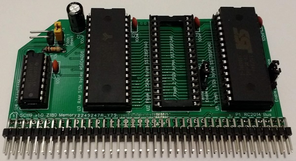
SC119 is a memory module for use with the Z180 CPU. It contains 2 x 512k bytes of Flash and 512k bytes of RAM.
A later design is now available: SC721

Documentation
- SC119 – Assembly guide
- SC119 – Circuit Explained
- SC119 – Firmware (see SC111)
- SC119 – Parts list
- SC119 – Printed circuit board
- SC119 – User guide
Downloads
Suppliers
| Kit Suppliers | Website | Ships from |
| Discontinued | ||
| PCB Suppliers | Website | Ships from |
| Small Computers Direct | SCDirect | UK |
| Stephen C Cousins | Tindie | UK |
| pcb4diy | pcb4diy.de | Germany |
| pcb4diy | eBay | Germany |
| Assembled and Tested | Website | Ships from |
| Not available | ||
| Component Suppliers | ||
| See parts list |
Older Versions
- none
Description
SC119 is a memory module designed to work with the Z180 CPU.
The module contains two 512k byte Flash ROM chips and one 512k byte RAM chip. Only one of the Flash ROM chips can be mapped into memory at any given time.
A jumper, or external switch, selects which of the Flash ROM chips is used. Alternatively, an external control signal could be connected to the switch header and used to control selection. By this method it would be possible to access all 1024k bytes of Flash memory.
The memory is organised in a 1M byte linear memory space. In order for a Z80 family CPU to access 1M byte of memory, some form of memory management (eg. paging) is required. As this module does not include such a feature, memory management must be provided elsewhere. The Z180 CPU includes a suitable memory management, but the standard Z80 CPU does not.
While it is possible to build a Z80 module with on-board memory management hardware, it is assumed this memory module will be used with a Z180 CPU, such as SC111.

The Flash memory supports being written to by the CPU, thus allowing the firmware to be updated, or “Flashed”. This is unlikely to happen by accident due to the software requirements for writing to the Flash, but to play safe each Flash chip has a jumper to select hardware write protection.
User Guide
Using SC119, v1.0, Z180 Memory module is pretty straight forward.
The module is designed to work with a Z180 processor, such as SC111, with the Z180 processor providing the memory management functions. The module has two Flash memory sockets to supports two sets of firmware, with a simple jumper or switch selection.

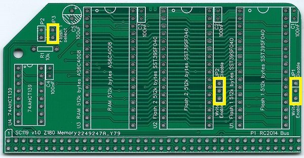
The module only has three jumper options.
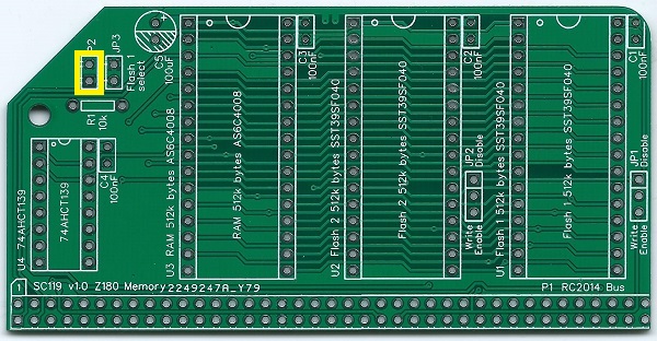
Jumper 3, shown below in yellow, selects which of the two Flash chips is used. Fit the jumper shunt to select Flash 1 (U1) or remove the shunt to select Flash 2 (U2).

The angled header pin (P2) next to JP3 allows connection of an external switch to select which Flash chip is used. It is possible to connect an external control signal to this header to allow software selection of the current Flash chip. This, in theory, allows access to 1M byte of Flash memory.
Jumpers, JP1 and JP2, shown below in yellow, enable each Flash chip to be independently write protected. It is unlikely the Flash chip will be corrupted in normal operation, due to the software requirements to write to it. However, for peace of mind you can disable writing with jumper shunts.

Each Flash chip has its own write protection jumper. Fit the shunt in the position shown below in green to disable writing. Alternatively, fit the shunt in the position shown below in red to enable writing.

In normal use it would be sensible to disable writing to the Flash chips, so set both shunts to the green position.
Parts List
| Reference | Qty | Component |
| PCB | 1 | SC119, v1.0, PCB |
| C1 to C4 | 4 | Capacitor, ceramic, 100 nF |
| C5 | 1 | Capacitor, electrolytic, 100 µF |
| JP1 and JP2 | 2 | Header, male, 1 x 3 pin, straight |
| JP3 | 1 | Header, male, 1 x 2 pin, straight |
| JP1 to JP3 | 3 | Jumper shunt |
| P1 | 1 | Header, male, 2 x 39 pin, angled |
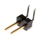
| P2 | 1 | Header, male, 1 x 2 pin, angled |
| R1 | 1 | Resistor, 10k, 0.25W |
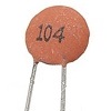
| U1 | 1 | SST39SF040, 512k byte Flash |
| U1 socket | 1 | 32-pin DIP socket |
| U2 | 1 | SST39SF040, 512k byte Flash |
| U2 socket | 1 | 32-pin DIP socket |
| U3 | 1 | AS6C4008, 512k byte SRAM |
| U3 socket | 1 | 32-pin DIP socket |
| U4 | 1 | 74AHCT139 |
| U4 socket | 1 | 16-pin DIP socket |
Printed Circuit Board


| Supplier | Website | Ships from |
| Stephen C Cousins | Tindie | UK |
| pcb4diy | eBay | Germany |
| pcb4diy | pcb4diy.de | Germany |
Assembly Guide
Experienced builders can just go ahead and populate the board. There shouldn’t be any surprises to catch you out.
This guide assumes you are familiar with assembling circuit boards, soldering, and cleaning. If not, it is recommended you read some of the guides on the internet before continuing.
First check you have all the required components.
Before assembling it is worth visually inspecting the circuit board for anything that looks out of place, such as mechanical damage or apparent manufacturing defects.
If you have a multimeter that measures resistance or has a continuity test function, check there is not a short on the power supply tracks. Connect the probes to each terminal of one of the capacitors, such as C1. This should be an open circuit, not a short.
The picture below shows what a completed SC119 Z180 Memory Module should look like.
Resistor
Fit and solder the 10k resistor R1 (shown in yellow below).
These can be fitted either way round, as they are not polarity dependent.

IC sockets
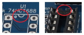
Fit and solder IC sockets for U1, U2, U3 and U4
Be sure to fit them with the notch matching the legend on the circuit board, so you do not end up fitting the IC the wrong way round too.
The sockets should be fitted in the positions shown below.

Capacitors
Fit and solder capacitors C1 to C4.
These can be fitted either way round, as they are not polarity dependent.

Bus Connector
Fit and solder bus connector P1.
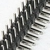
You may need to cut the connector strip to length (if starting with a strip more than 39 pins long). Long nose wire cutters snip through the plastic quite easily.
Take care to ensure the pins are parallel to the circuit board so that the board will be vertical when plugged into a backplane.

Header Pins
Fit and solder the right-angled male header pins, P2.
Take care to ensure the pins are parallel to the circuit board.
Jumper Pins
Fit and solder the jumper pins for JP1 to JP2.
Each of these is a single, 1 row by 3 pin header.

Fit and solder the jumper pins for JP1 and JP2.
JP3 is a single, 1 row by 2 pin header.

Capacitor
Fit and solder electrolytic capacitor C5.
It is important to fit this capacitor the right way round. The negative terminal is indicated with a ‘minus’ sign, as illustrated to the right. The negative terminal also has a shorter lead.
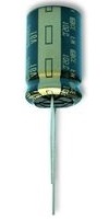
The capacitor is fitted in the position illustrated below, with the negative terminal at the bottom (hashed area) and the positive at the top (marked with a ‘plus’ symbol.

At this component is quite tall, it might be worth bending the leads such that the capacitor lays flat against the board, in the position indicated below. This avoids the possibility of it touching the next board on the backplane.

Inspection
Remove any solder ‘splats’ with a brush, such as an old toothbrush.
Visually inspect the soldering for dry joints and shorts.
Clean the flux off with suitable cleaning materials.
Visually inspect again.
Before fitting the ICs, plug the board into an RC2014 backplane with no other boards fitted. Power the backplane and perform the following check with a voltmeter:
- Check the supply voltage on the memory module, between, say, U4 pin 8 and U4 pin 16. This should be 4.5 to 5.5 volts, preferably 4.75 to 5.25 volts.
If all is well, power down and remove the memory module.
Integrated Circuits
Insert the ICs into their sockets, taking care to insert them the correct way round, as illustrated below. Be careful not to bend any legs over.

Test
Fit jumper shunts in the positions indicated below.
JP1 and JP1 shunts are positioned to write protect the Flash memory.
JP3 is fitted to select Flash chip 1 (U1). To select Flash chip 2 (U2), remove the jumper shunt.

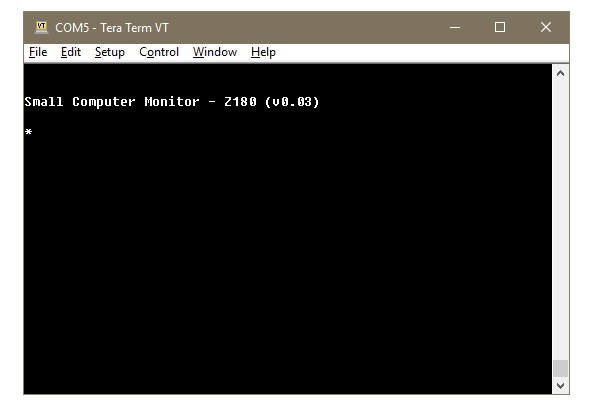
The following assumes you are using the Z180 CPU module SC111 and have the Small Computer Monitor, configuration S5, installed in socket U1 of this memory module. Jumper shunt JP3 should be fitted to select Flash chip 1 (U1).
Fit this module to a suitable backplane, along with the Z180 CPU module. Connect an FTDI style 5 volt serial cable to the CPU module’s serial port A, with the other end connected to a computer running a terminal emulation program. The terminal should be configured for 115200 baud, 8 data, 1 stop, no parity. Flow control can be either Off, or hardware RTS/CTS.
Turn the power on to the system. The terminal should show something similar to the illustration below.
Circuit Explained
The SC119, Z180 Memory module includes the two 512k byte Flash chips and one 512k byte RAM chip. In normal operation, only one of the Flash chips can be used, meaning the module effectively provides 1M byte of memory (512k Flash, plus 512k RAM).
To create a minimal computer system, a Z180 CPU module must be added, together with a backplane to connect the two modules.
C1 to C4
These capacitors provide power supply decoupling (or bypass). The fast switching in digital circuits creates spikes on the power supply lines which are suppressed with decoupling capacitors placed at key points on the circuit board.
C5
This capacitor helps prevent the supply voltage from dipping when current surges occur.
JP1 and JP2
Jumper 1 allows Flash chip U1’s write enable input to be connected to either Vcc (5 volts) or the CPU’s write output (/WR). Jumper 2 provides the same function for Flash U2.
When the Flash chip’s write enable input is connected to Vcc, the Flash chip will never get a write enable signal and thus the memory is protected against being changed. When connected to the CPU’s write output, it is possible to write to the Flash chip.
Writing to the Flash chip is unlikely to happen by accident due to the software requirements. However, for peace of mind it is generally best to disable writing with this jumper.
JP3
When a jumper shunt is fitted to this header, Flash U1 is selected. When the shunt is not fitted, Flash U2 is selected.
Header pins P2 allow an external switch to be used instead of a jumper shunt. In addition, it is possible to connect and external control signal to this header to enable software selection of the current Flash chip. By this method it is theoretically possible to access both Flash chips.
The external signal is a simple digital level, low for U1 and high for U2. There is a pull up resistor on this signal, so it defaults to high when not connected.
U1 and U2
These are 512k byte Flash memory chips.
U3
This is a 512k byte static RAM chip.
U4
U4 is a dual 2-to-4 line decoder. This handles address decoding for the memory. The Z180 has a 1M byte memory map. The bottom 512k bytes is decoded to the currently selected Flash chip, while the top 512k bytes is always the 512k byte RAM chip.
A 74AHCT139 is specified instead of the usual HCT series component. The AHCT part is faster, thus increasing the chances of being able to run the system at a higher clock speed than the default 18.432 MHz. In fact, the Z180’s software selectable clock multiplier could be used to overclock the system to 36.864 MHz. However, I must stress that this is NOT in any way guaranteed to work.
P1
This is the RC2014 bus connector.
P2
This is a header to connect an optional external flash chip select switch, as described above.
Notes
- This design is made in accordance with the “designed for RC2014” labelling scheme.
- RC2014 is a trademark of RFC2795 Ltd.
- This product is designed for hobby use and is not suitable for industrial, commercial or safety-critical applications.
- The product contains small parts and is not suitable for young children.
