SC500 Series: Jumper Settings

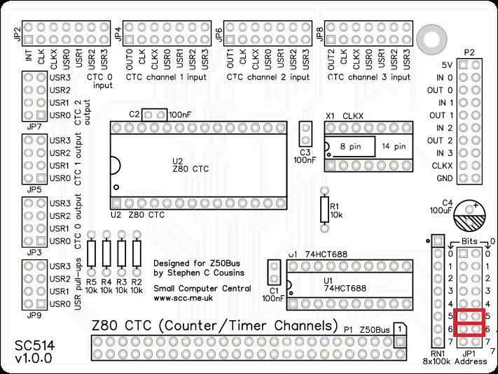
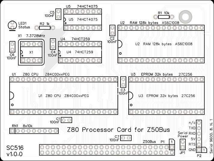
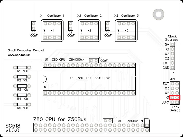
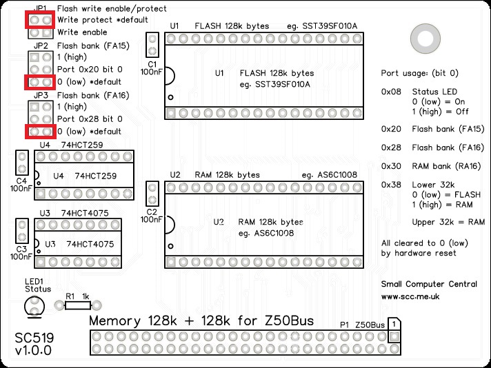
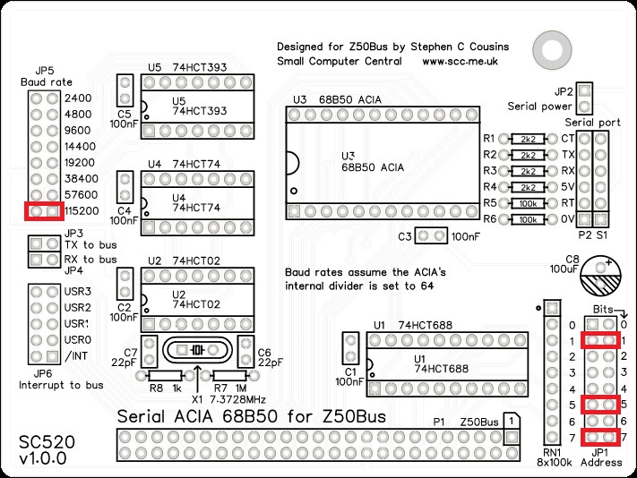
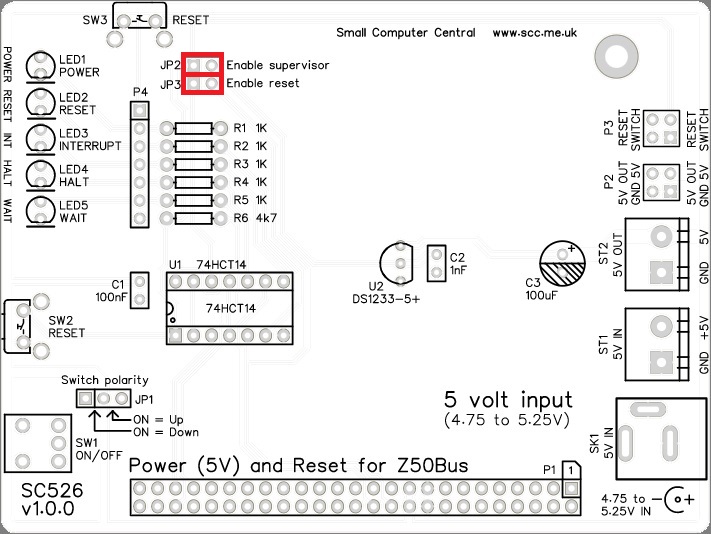
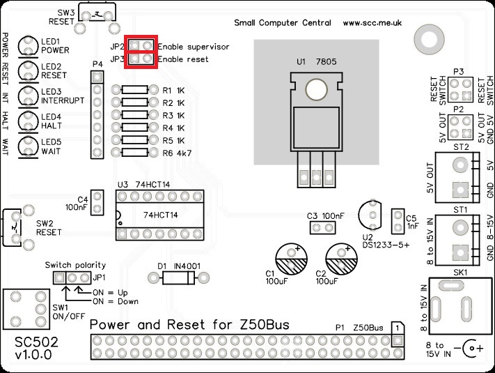
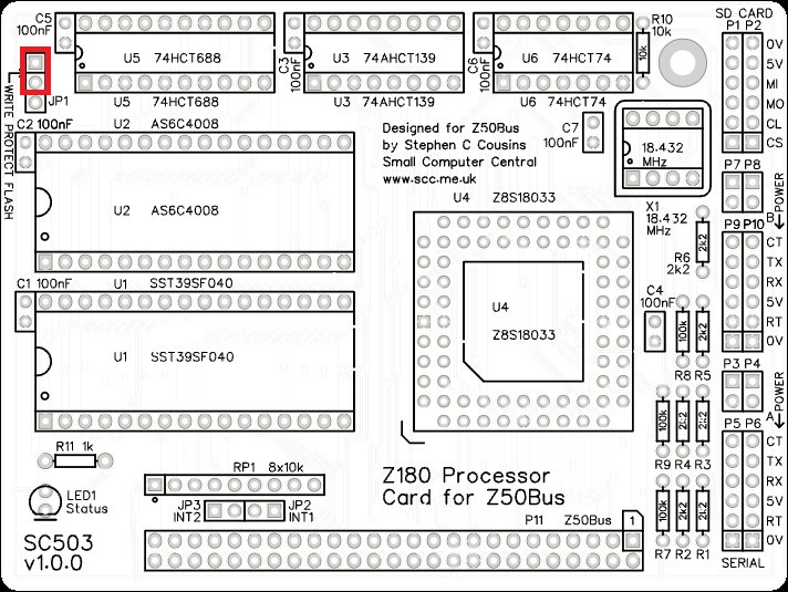
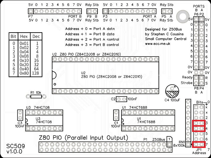
The illustrations below show the recommended default jumper shunt positions for each card.

Currently, some software and firmware require different settings, so always check the settings required by the software and firmware you are using. Known exceptions are listed below each image.

SC502 – Power and Reset Card
SC503 – Z80 Processor Card
SC504 – Compact Flash Interface Card – Address 0x90
SC505 – Real-Time Clock and I2C Card – Address 0x0C
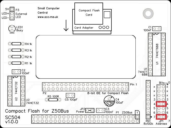
This should be 0xA1 to best meet the Z50Bus guidelines
SC506 – Digital Input/Output Card – Address 0xA0
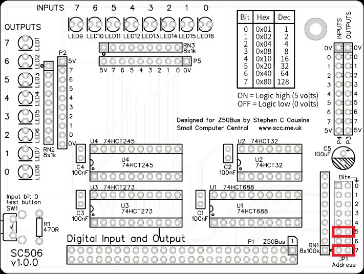
Exception: RomWBW v3.0.1 2021-10-24, Address 0x0D
SC509 – Z80 PIO (Parallel Input/Output) – Address 0x98
SC511 – Z80 SIO (Serial Input/Output) – Address 0x80
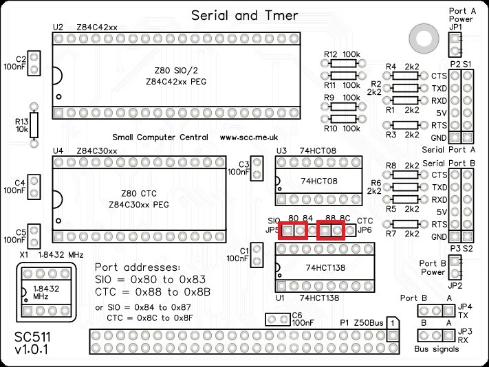
and Z80 CTC (Counter/Timer Channels) – Address 0x88
Exception: RomWBW v3.0.1 2021-10-24 does not support this card, dev branch should work
SC514 – Z80 CTC (Counter/Timer Channels) – Address 0x60
SC516 – Z80 Processor Card – Default is no jumper shunts
SC518 – Z80 CPU (Central Processor Unit) – Clock source = oscillator 1
SC519 – Z80 Memory (128k+128k) – Default Bank Selection
SC520 – Serial ACIA (68B50) – Baud rate = 115200 baud – Address 0xA2
SC521 – Z80 SIO/2 – Clock source = X2, baud rates = 115200 baud – Address 0x80
SC523 – Programmable ROM – Write protected, bank zero selected
SC526 – Power and reset – Reset and supervisor enabled
SC527 – Z80 processor – Oscillator X2, Flash protected,Flash bank zero selected

Homebrew 8-bit retro computing